Image transfer, also known as photolithography (or simply, lithography), plays a crucial role in defining the circuit patterns on a panel. With photolithography, IC substrate manufacturers can construct intricate and precise connections required to support more connectivity over a smaller area.
With demand increasing for higher circuit density and narrowing distances between lines, copper traces must be formed with extreme precision and uniformity.

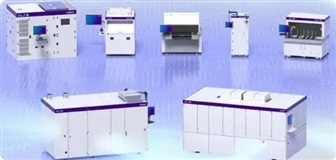
KLA's direct imaging solutions for patterning systems.
Specifically for semiconductor advanced packaging applications, a wide range of advanced IC substrates such as multistrip flip chip-chip size package (FCCSP) and flip chip ball grid array (FCBGA) require high resolution and accurate lithography. For advanced IC substrates – characterized by large unit size, high layer count, and fine lines – patterning poses unique challenges for manufacturers, especially when it comes to imaging on uneven topography. IC substrate manufacturers must pattern extremely thin features that require exceptional registration and overlay accuracy.
Broadly speaking, manufacturers face three key challenges:
1. Achieving smooth fine traces without stitching
2. Improving layer-to-layer alignment for accuracy
3. Maintaining high productivity and efficiency
IC Substrate Line Quality
As IC substrate architecture complexity increases, with more layers and bigger bodies, distortion across the x-y axes and topography variation (z-axis) pose significant challenges for IC substrate manufacturing. More specifically, when imaging advanced substrate layers, stitching issues (i.e., line/traces shift or deviation) are compounded by surface irregularities leading to yield penalty.

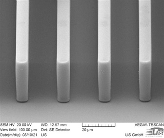
Super-fine, highly uniform lines with outstanding accuracy are required for advanced panel technologies.

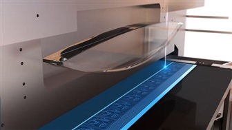
Advanced optics systems are required to overcome challenges.
Both challenges cannot be fully addressed by existing solutions such as digital micromirror devices (DMD), direct imaging (DI), and steppers. High and continuous depth of focus (DOF) and advanced compensation mechanisms are necessary to overcome both.
Moreover, for high-frequency applications, linewidth uniformity and edge roughness pose additional challenges, as maintaining trace uniformity is key to optimal transmission and signal integrity.
Layer-to-Layer Alignment for Higher Accuracy
As package functionality increases, optimized layer-to-layer alignment is imperative to enable more input/output (and consequently, bumps) through smaller pad designs. It can be achieved by implementing advanced scaling algorithms and a high-precision platform. All the while, alignment optimization must not impact substrate dimensions.

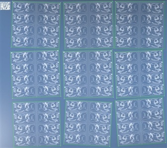
Scaling algorithms can help achieve optimized layer-to-layer alignment.
Productivity and Efficiency
Productivity and efficiency are key to short time-to-market and low cost of ownership. Increasing the number of strips or partitions, especially in advanced FC-CSPs and modules, leads to a reduction in system productivity and an increase in manufacturing costs. In addition, for advanced FC-BGA, where steppers are currently the main patterning solutions in use, masks are required, leading to a longer time to market and significant costs.
The KLA Approach to IC Substrate Photolithography
KLA's portfolio includes multiple direct imaging solutions, designed to address the lithography challenges of today and tomorrow. Market adoption of KLA's Corus™ direct imaging platform demonstrates its proven capability as a flexible and efficient imaging solution.
For advanced IC substrate applications, KLA's Serena™ platform has just been introduced, representing a new lithography category beyond steppers. This innovative digital solution is designed especially for fine-line patterning of large-sized, high-layer count organic substrates, delivering increased accuracy and yield.
Learn more about KLA's direct imaging solutions for IC substrates.

KLA's direct imaging solutions are part of the semiconductor industry's widest breadth of process control and process-enabling solutions for IC substrate manufacturing.
