


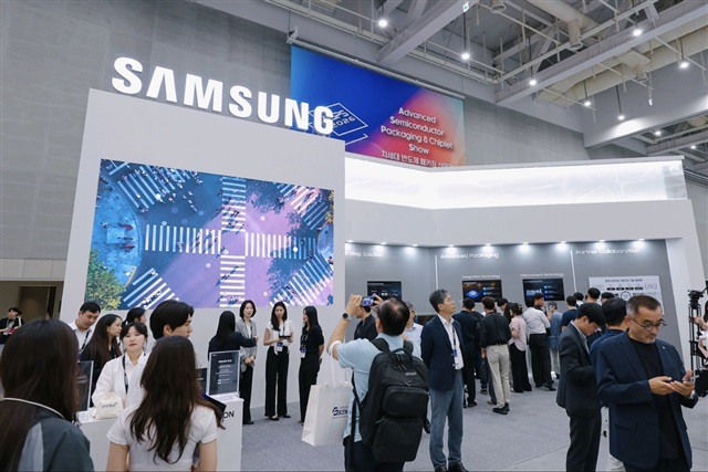
Samsung Electronics has opened an advanced packaging research center in Yokohama, bringing development work closer to Japanese suppliers that provide critical materials and equipment for high-bandwidth memory (HBM) as the company works to narrow its...
The article requires paid subscription.
Subscribe Now
