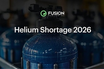
CONNECT WITH US
Thursday 30 October 2025
Asian Power Devices Officially Launches New Vietnam Factory, Setting a New Global Production Milestone
Taiwanese power solutions leader Asian Power Devices Inc. (hereafter "APD") officially inaugurated its new factory on October 29 at Thang Long Industrial Park in Phu Tho Province, Northern Vietnam. The event brought together APD's international clients and supply chain partners to witness this significant milestone in the company's global expansion. APD's Vietnam factory specializes in the production of power supply units, with mass production having commenced in September 2024 and full-scale capacity expansion planned for 2025
Thursday 20 November 2025
Henkel to Present Breakthrough Die Attach Technology in Upcoming Power Device Webinar
As the demand for high-performance power semiconductors continues to escalate across automotive and industrial sectors, Henkel is addressing one of the industry's most pressing challenges: thermal management in next-generation power devices.Henkel will host a technical webinar introducing its patented Polymerization-Induced Phase Separation technology platform-an advanced solution engineered to meet the evolving requirements of power device performance, reliability, and cost-efficiency.Thermal Control as a Critical EnablerWith rising operational temperatures directly impacting device reliability and efficiency, effective heat dissipation has become essential. The industry's transition to bare copper (Cu) designs-driven by cost and reliability considerations-further underscores the need for die attach materials that combine high thermal conductivity with Cu compatibility.Henkel's innovative technology enables die attach formulations that could meet automotive Grade 0 thermal cycling and MSL1 reliability standards; provide high bulk thermal conductivity for metallized or bare silicon die; ensure compatibility with a wide range of die finish and lead frame combinations, including bare copper; deliver improved RDS(on) performance compared to conventional die attach materials; support copper wire bonding processes. This event marks the first installment in Henkel's Power Device Webinar Series, designed to provide engineers, designers, and industry stakeholders with insights into materials innovations that address the increasing demands of power semiconductor applications.To particiapting in this webinar titled :"What's Powering the Next-Gen Power Device Performance" on 2025/11/28 10:00-10:45 am (Singaporean Time GMT+8), please register, click here to register.Participants will gain exclusive access to Henkel's technical experts and learn how this proprietary platform is setting new benchmarks in thermal performance and reliability for power devices.
Thursday 20 November 2025
Powering the AI Revolution: How MKS Is Shaping the Future of Electronics Manufacturing in Asia
When you walk the halls of the TPCA Show Taipei 2025, one theme is impossible to miss: AI is no longer the future-it's the engine driving the next great wave of electronics manufacturing. From cloud data centers to handheld devices, Artificial Intelligence is reshaping how the world processes information. And behind every AI-driven device is an intricate network of high-performance PCBs, advanced substrates, and precision manufacturing technologies.Reporter Gary with the MKS-Atotech leadership team, including the CEO. Credit: MKS-AtotechAt the center of this transformation stands MKS Instruments, whose strategic brands Atotech and ESI are powering the next chapter of Asia's semiconductor and advanced electronics industries.The New Frontier: AI and the Rise of Advanced PackagingAI's explosive growth has created a new set of demands: faster computing, higher data throughput, and unprecedented integration of components. The era of simple, monolithic chips is long gone. Today's AI processors rely on heterogeneous integration, where multiple chiplets are packaged together on complex organic substrates."It's a materials revolution," explains Dave Henry, Executive Vice President Global Strategic Marketing and GM, Materials Solutions Division. "Our technologies touch more than 70% of the critical steps in PCB and substrate manufacturing-and over 85% of semiconductor front-end processes. MKS is deeply embedded in the future of electronics."This new generation of packaging requires ultra-fine features, tighter interconnects, advanced metallization, and laser-drilled structures at microscopic scale. The PCB industry-particularly in Taiwan-is experiencing a surge in demand, driven by applications in AI, HPC, satellite communications, automotive electronics, and beyond.Inside the MKS Booth: Where Chemistry Meets Systems Technology: From Via Drilling Lasers to horizontal and vertical chemical process equipmentOne of the busiest destinations at TPCA 2025 was the MKS booth, where crowds gathered to explore a unique, fully integrated portfolio: lasers, chemistry, plating systems, motion control, optics, software, and more.MKS is one of the few companies in the world capable of delivering this level of end-to-end process integration. Its Atotech and ESI brands showcased side-by-side how laser drilling, surface treatment chemistry, plating systems, and advanced software work together to Optimize the InterconnectSM—a strategic approach to enabling next-generation electronics.This unified offering is more than convenient-it's transformational"AI chips require high-speed interconnects, smaller geometries, and new substrate materials," says Harald Ahnert, Vice President and GM of Chemistry. "Our solutions bring together decades of expertise to help customers manufacture these advanced products at scale."Spotlight on Innovation: The Technologies Everyone Was Talking AboutA walk through the MKS booth was a look into the future of electronics manufacturing, with several standout technologies drawing sustained attention from visitors.One major area of focus was breakthrough chemistry for advanced substrates. MKS highlighted InPro Pulse TGV, designed for high-aspect-ratio through-glass vias, alongside Cuprapulse IN, a reverse-pulse plating solution developed for HDI and package substrates. For reliable final finishing, the company showcased Aurotech G-Bond 3, Stannatech 2100, and PD Core, complemented by EcoFlash S300U, Bondfilm EX, and Novabond PX-S2, which support high-speed, low-loss signal integrity. Taken together, these chemistry solutions cover a broad spectrum of manufacturing needs, from SAP and SLP production to ultra-fine line formation down to 2/2 μm.Another highlight was the portfolio of next-generation equipment systems. G-Plate was presented as a solution for high-volume PTH processing with capability below 5/5 μm, while vPlate offered continuous vertical plating with industry-leading uniformity. Uniplate platforms were positioned as robust systems for mass production of HDI PCBs, and the PLB Line was specifically engineered to meet the demanding requirements of AI server boards. Combined, these systems form a core platform for the future of PCB and substrate fabrication.The ESI brand further elevated the booth with cutting-edge laser systems. Capstone was featured for high-throughput UV flex drilling, Geode A demonstrated precision CO? processing of ABF laminates, and Geode G2 showcased ultra-fast via drilling for HDI and mSAP applications. "The industry is facing growing complexity: more I/O, more drilling, more layers," says Michael Stubelt, VP and GM of Equipment Solutions. "Our laser systems give manufacturers the flexibility and productivity advantage they need."Why Glass Substrates Are the Next Big ThingOne of the most talked-about highlights at the show was a striking, panel-scale processed glass substrate sample on display at the MKS booth. Glass, once considered exotic, is fast gaining traction as the next major substrate material in heterogeneous integration.MKS is developing complete process flows for glass—including surface preparation, seed-layer formation, metallization, and via filling—combining Atotech chemistry with ESI's high-speed laser drilling. This collaboration reflects a broader theme: MKS doesn't just deliver tools; it builds ecosystems.Scaling Up: New Investments Across Southeast AsiaWhile the spotlight was on technology, MKS also shared details of its expanding regional footprint. "Competition in APAC and Greater China is intense," says George Yang, VP and GM for MKS Greater China. "Our strategy is to be local—local manufacturing, local tech support, local expertise." Today, MKS operates 14 manufacturing sites across the APAC region and is investing aggressively in Southeast Asia.One of the major new investments is a Super Center for wafer fabrication equipment in Penang, Malaysia, which has been under construction since 2024. In Samut Prakan, Thailand, the company has recently opened a Tech Center and manufacturing site dedicated to PCB and substrate development, further strengthening its presence in advanced electronics manufacturing.MKS is also moving ahead with a flagship expansion in Thailand. In May 2025, the company broke ground on a new Atotech chemical manufacturing facility and Tech Center near Bangkok, representing an investment of more than US$40 million. The site is designed for an annual capacity of 18,500 tons and is scheduled to begin operations in the second half of 2027. As Thailand rapidly emerges as a major PCB manufacturing hub and attracts investments from China, Korea, Taiwan, and Japan, MKS aims to be a pillar in this fast-growing ecosystem.The Road Ahead: Enabling the Electronics of TomorrowFrom semiconductors and substrates to optical systems and laser drilling, MKS Instruments touches nearly every step in the electronics manufacturing chain. Its integrated approach—rooted in deep expertise across materials science and precision engineering—provides customers with the tools needed to build faster, more compact, more efficient AI hardware."MKS is proud to contribute to the industry's move toward advanced and eco-friendly manufacturing," says Wayne Cole, Senior Vice President of Global Sales and Service. "Our mission is to help customers stay competitive in a world that is evolving faster than ever."With major investments across Southeast Asia, a powerful portfolio of technologies, and a unified vision MKS is not just participating in the AI revolution-it is helping to build the foundation on which the future of electronics is being created.MKS is enabling the shift from transistor scaling to advanced integration - merging logic, memory, and photonics. The company's APAC Tech Centers act as co-innovation hubs for customers, encompassing: supporting R&D, process training, and sub-5/5 µm SAP prototyping.These centers are not just service nodes - they're bridges between customer vision and manufacturing reality.MKS has a proud history of innovations and inventions that have shaped the evolution of the key industries we serve. As a global leader in providing equipment, processes, and production solutions that power the most advanced electronic devices, our expansion in Asia reflects our commitment to supporting the growth of the semiconductor, PCB, and package substrate markets in this region. We are excited to be a key player in the future of technology and look forward to continuing to invest in Asia's bright future.  Reporter Gary interviewed the MKS-Atotech leadership team at TPCA Show 2025. Credit: MKS-Atotech
Tuesday 18 November 2025
PGC Strengthens Cloud and AI ASIC Acceleration with Synopsys' Next-Generation Interface and Memory IP on Advanced Nodes
As AI workloads scale across global cloud infrastructure, chip designers face a persistent challenge: balancing compute throughput, bandwidth, and power efficiency amid escalating design complexity.Emerging architectures built around UCIe-based chiplets, PCI Express 7.0 and CXL 3.1 interconnects, and 2.5D/3D memory-integrated packaging have made integration-not computation-the new bottleneck.Progate Group Corporation (PGC, TPEx: 8227), a member of TSMC DCA, leverages its long-term partnership with Synopsys to solve that bottleneck.Through a unified ASIC turnkey flow, PGC enables innovators to design, verify, and manufacture advanced-node SoCs and chiplet-based accelerators for cloud and AI applications with greater efficiency and lower risk.PGC integrates the latest generation of Synopsys Interface IP, spanning high-speed interconnects, memory, and networking subsystems critical to modern cloud and AI processors.The portfolio includes UCIe 40G Die-to-Die, CXL 3.x, and PCI Express 7.0 controllers that enable seamless chiplet-based compute integration for next-generation server processors.It also incorporates HBM4 and DDR5 Gen2 memory subsystems optimized for multi-stack 2.5D and 3D integration, as well as 224G Ultra Ethernet PHY solutions designed for high-throughput data-center networking.Validated across TSMC 3nm to 2nm process nodes, these silicon-proven IPs address the cloud industry's most demanding bandwidth and power-efficiency challenges while maintaining full compatibility with Synopsys EDA and PDK environments.Through its TSMC Design Center Alliance (DCA) membership, PGC provides a verified turnkey service covering RTL design, APR layout, wafer fabrication, 2.5D/3D packaging, and final test coordination.By integrating Synopsys EDA tools (Design Compiler, Fusion Compiler, ICC2, PrimeTime) and complete IP deliverables (Lib, LEF, GDS, and testbench models), PGC helps customers accelerate RTL-to-signoff cycles through pre-verified IP subsystems, SIPI (signal and power integrity) analysis, and IP hardening support-as described in Synopsys' IP Accelerated methodology.This unified approach reduces integration risk, minimiclozes manual iteration, and ensures design closure consistency across advanced-node ASIC projects."Cloud and AI systems are evolving into distributed compute platforms built on multiple dies and protocol layers," said Fred Lai, CEO of PGC."By aligning Synopsys' IP Accelerated methodology with TSMC's leading-edge processes, PGC helps customers scale performance while maintaining design predictability and manufacturing reliability."Unlike large turnkey providers that concentrate solely on a handful of mega-scale clients, PGC combines advanced-node design capability with engineering agility, making it a trusted partner for both hyperscalers and rapidly growing AI startups.Beyond simplifying multi-vendor coordination, the company maintains unified technical accountability across design, IP integration, and manufacturing, ensuring that every stage of development proceeds seamlessly.PGC's engineers perform SIPI co-optimization using Synopsys EDA and PDK models to guarantee signal and power stability, while TSMC-certified signoff flows deliver predictable yield and reliability.Supported by cross-regional teams in Taiwan, Japan, China, and the United States, PGC provides rapid collaboration and execution across the entire ASIC turnkey cycle.PGC's ecosystem extends from design integration to manufacturing, combining TSMC's advanced-node foundry services, Synopsys' comprehensive IP portfolio, and partnerships with leading OSAT partners for 2.5D/3D packaging enablement.Together, this network provides a complete foundation for high-bandwidth, energy-efficient ASIC innovation across AI, HPC, and cloud computing markets.