SEMICON Taiwan 2024 featured the latest trends and innovations that focused on the future of Artificial Intelligence (AI) to connect Taiwan and global semiconductor ecosystems. The high demand and getting larger-sized AI chips require advanced packaging technologies to improve performance and time to market while reducing chip manufacturing costs and power consumption. The heterogeneous integration including 2.5D, 3D hybrid bonding, fan-out, and system-on-a-chip (SoC) packaging, along with emerging solutions like silicon photonics and panel-level packaging, are critical in optimizing system performance. These trending technologies are offering a higher-value opportunity and propelling the global semiconductor industry to foster the big waves of AI and high-performance computing chip innovation.
The chemical solution providers play an important role in helping chip makers develop and commercializing various advanced packaging solutions to win premium customers. In this exclusive interview in the private conference room of SEMICON Taiwan with Mr. Ramachandran (Ram) Trichur, Global Market & Strategy Head for Semiconductor Packaging at Henkel Adhesive Technologies Electronics. He started recap the market observation of the semiconductor industry in 2024Henkel Adhesive Technologies business unit is the global leading chemical solution provider for adhesives, sealants, and functional coatings with sales of EUR10.790 billion in fiscal 2023. Henkel is the premier materials supplier for the electronics assembly and semiconductor packaging industries.

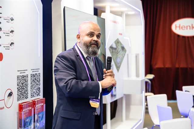
Mr. Ramachandran (Ram) Trichur, Global Market & Strategy Head for Semiconductor Packaging at Henkel Adhesive Technologies Electronics.
Expecting AI killer applications drive massive growth for edge computing
Ram described the market as in a persistently challenging business environment as well as the market recovery in the Electronics business in 2024. Especially the advanced packaging is now gaining significant momentum as the next pathway for breakthroughs in semiconductor technology. The company expects single-digit market growth for 2024 and is optimistic about looking into 2025 as a massive increase in demand for the semiconductor market.
He has observed several notable trends. First of all, in the past two years, generative AI has rapidly evolved and driven cloud computing AI revenue growth for enterprises. However, the volume of AI-enabled electronic devices is not increasing in the same way currently. The chip makers and electronic manufacturing industry are looking for applications to drive the unit count growth happened in the edge computing AI sector.
Meanwhile, consumer electronics brands have quickly responded to promote their latest AI-powered products to figure out how consumers use AI to expand use cases that people use every day. There are more AI-enabled devices coming. Nowadays, some newly released fancy devices including AI personal computers (PC), AI smartphones, and intelligent robotics in automation systems are gathering attention. While companies race to incorporate AI technologies internally and externally, consumer use of AI still requires more time to see the results.

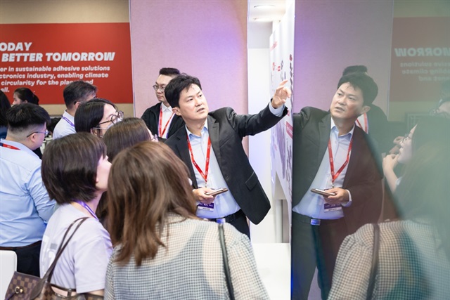
Henkel hospitality suite showcasing solutions at SEMICON Taiwan 2024
Photo: Henkel
Thermal mechanical challenges in advanced packaging
Semiconductor chips are essential for the development and deployment of AI at scale. There are several primary challenges to be tackled in the semiconductor industry. Thermal-induced mechanical stress is now one of the leading causes of semiconductor failures, and it is becoming a top focus for chip manufacturers and ecosystem partners. "The bigger chips mechanically have big space and cause warpage and stress issues happened while ICs in operation," said Ram. He acknowledges the control of the warpage or mechanical stress to prevent chip failure is the highest priority for both material providers and chip manufacturers. The collaboration of ecosystem partners jointly developed and set a guideline on the maximum warpage or stress allowed in 3D-ICs, and designers could follow and avoid exceeding the constraints.
Henkel is focusing on providing semiconductor packaging materials with long-term reliability, optimized performance, and processability for high throughput production. The demonstrated chemical solution lineups in SEMICON Taiwan 2024 include several major categories of advanced packaging materials. They are advanced underfill, non-conductive pastes & films (NCP & NCF), wafer-level encapsulation, and lid & stiffener attach materials.
Lid & stiffener adhesives strengthening, warpage-reducing, grounding or shielding
Ram divided the use of Henkel's materials for 2.5D/3D integrated packages in the manufacturing process into several highlights. The first is the lid & stiffener attach materials. The metal parts of lid & stiffener design in the larger-sized packaging is useful to reduce warpage concerns while dealing with tighter interconnects, thinner dies, complex architectures, and multiple coefficients of thermal expansion (CTE) in a single package. The Henkel's semiconductor adhesives are reliably attached to the lid and peripheral stiffeners to the substrate, allowing the package to maintain flatness throughout production and operational thermal cycles.
During the manufacturing process and in operation, these devices and their multiple dies are subjected to several thermal cycles which can stress interconnects, leading to warpage and mechanical damage. The design of Henkel's lid & stiffener attach materials provides a portfolio of stability-enhancing adhesives ranging from conductive and non-conductive formulations, providing warpage-reducing coplanarity as well as grounding or shielding capability.
Large die capillary underfill considering bump protection and warpage control
The second highlight is focusing on advanced underfill materials. The 3D-IC design continues to increase the silicon interposer area to accommodate multiple dies including memory and processor units allowing the dense die integration inherent in advanced packaging techniques. This will require the underfill material with low shrinkage and toughness to provide die and underfill crack resistance, while its low coefficient of thermal expansion (CTE) protects against warpage. Targeting to meet the dimensional demands of highly integrated package designs, Henkel's Capillary Underfill(CUF) materials completely envelop fine-pitch, low gap height die interconnects for rigid protection against stress to deliver good electrical, moisture, and thermal reliability performance for high production yields.
However, there is rising processability or manufacturing throughput requirements while the Capillary Flow Materials fill a large area in the substrate for bigger ICs. The flow speed allowing for greater process efficiency is an important feature for complete interconnect coverage. Henkel takes a quick response to release new materials. Taking Loctite Eccobond UF 9000AE as an example, in internal testing versus previous generation Capillary Underfills, Loctite Eccobond UF 9000AE demonstrated 20% faster flow on a 40 mm x 40 mm die, indicating that this material is compatible with even larger die sizes. So far, Loctite Eccobond UF 9000AE's performance has been validated on die as large as 50 mm x 50 mm and within packages up to 110 mm x 110 mm.
Liquid compression molding materials support high reliability & high-UPH process
The third highlight is advanced molding and encapsulation materials. Wafer-level packaging shows significant growth potential, chemical solutions including advanced molding and encapsulation are enabling accelerated adoption by providing improved handling, protection, and warpage control for thinner die design approach. The challenges are the molding area is getting larger and the molding thickness is thin. The warpage becomes large after curing and it affects proceed to the subsequent process. Henkel's portfolio of wafer-level encapsulation materials include a variety of solutions to facilitate high-yield processing and in-field reliability for various advanced wafer-level packaging applications. The focus of the demo section is liquid compression molding materials (LCM).
Henkel's liquid compression molding materials for wafer-level packaging processes integrate ultra-fine filler technology (less than 10 μm upper-cut) to deliver void-free gap filling and thorough coverage. In addition, the high warpage control and fast in-mold curing of Henkel's formulations molding materials provide high reliability in combination with a high-throughput process for overall lower cost. The LCM materials are anhydride-free and REACH-compliant, ensuring that the die remains protected under various operational stresses.

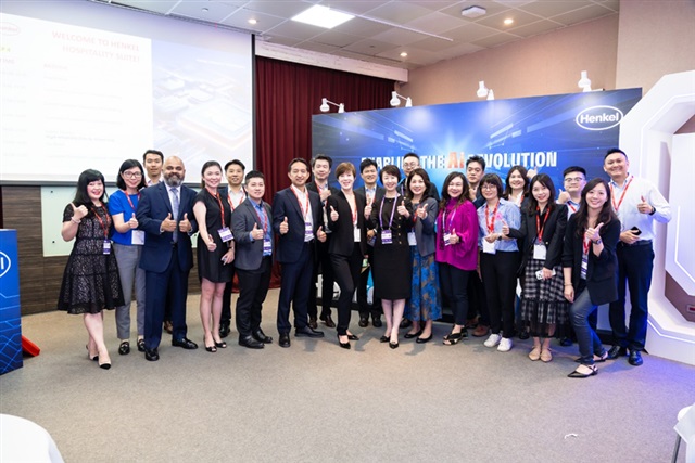
Henkel Adhesive Technologies Electronics
Photo: Henkel
Henkel Taiwan Electronics Adhesives Technical Center supports customers' technology roadmaps
Henkel is well positioned to deliver the sustainable high-performance materials needed for next-generation advanced packaging. These series of Henkel's solutions offer characteristics with high reliability, thermal expansion, fast capillary flow to satisfy the requirements of complex, high-density semiconductor packages. In all product developments, Henkel's sustainability commitments to use renewable carbon content and eliminate Substances of Very High Concern (SVHC) materials will remain a priority. The newest generation of advanced packaging is integrated with the technologies with environmental protection and partnerships with industry leaders. This will drive the material innovation to satisfy the semiconductor manufacturing fab requirements.
There are more versatile and potential opportunities for semiconductor advanced packaging technology underway including Co-Package Optics (CPO), panel-level packaging, and other emerging techniques. The next steps for Henkel Adhesive Technologies will continue investing heavily in material innovation and seek to understand the evolving needs of the semiconductor and electronic materials market while actively proposing chemical products that align with customers' technology roadmaps and contributing to the research and development of new products.
Moreover, Henkel Taiwan Electronics Adhesives Technical Center at Zhubei City provides prompt technical support and increases collaboration with Taiwan customers to speed up prototype development. This application center is dedicated to supporting customers in technical innovation and product development through faster application simulation, data generation, and analysis, thereby accelerating time-to-market for advanced packaging technologies. Ram concludes, "Through Henkel's dedicated global support teams and in close partnership with customers, Henkel Adhesive Technologies will create technical breakthroughs to open a new frontier for semiconductor advanced packaging."

