
ASIP Technologies will focus its Visakhapatnam semiconductor facility on flip-chip ball grid array packaging as it works toward volume production in the fourth quarter of 2027, Managing Director and CEO Venkata Simhadri told DIGITIMES.
The company expects South Korean technology partner APACT to support the plant's setup and train its first group of production staff. ASIP plans to ramp the facility to its annual capacity of 96 million chips within 1-2 years after operations begin.
"Our goal is to get into volume production by Q4, 2027," Simhadri said. "It is an aggressive schedule, but projects in other countries have done that."
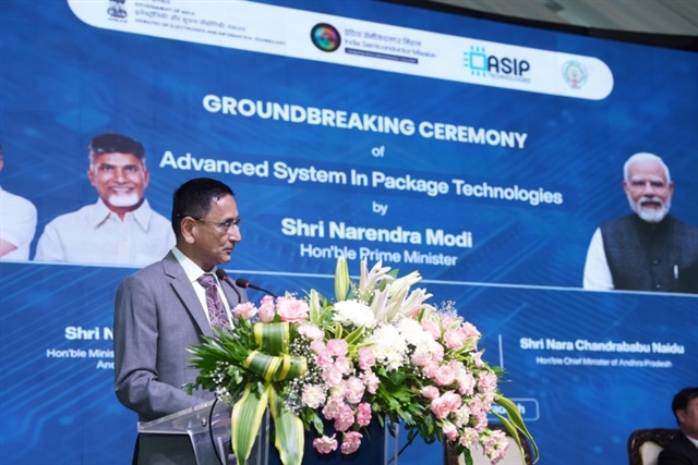
Prime Minister Narendra Modi virtually laid the foundation stone for the project on August 1. The facility is being built on a 30-acre site at Tarluvada in Visakhapatnam, Andhra Pradesh.
FCBGA to lead initial package mix
ASIP will primarily offer FCBGA packaging for system-on-chip (SoC) products used in networking, communications and computing. Consumer electronics will also be among the target markets.
FCBGA packages use a flip-chip connection between the semiconductor die and substrate. The approach is commonly used for chips that require higher input-output density than conventional wire-bond packages can provide.
The Visakhapatnam plant will have a smaller wire-bond operation serving power electronics, automotive and consumer applications, Simhadri said.
ASIP has also announced plans to introduce 2.5D and 3D packaging within two to three years of starting production. It has not disclosed the planned capacity for those processes. The company's near-term priority, however, is to install and qualify the initial FCBGA and wire-bond lines before the end of 2027.
APACT to support equipment and line setup
APACT will advise ASIP on its packaging portfolio and equipment selection. The Korean OSAT company will also assist with installation and the process of bringing the assembly lines into operation.
Simhadri said APACT's experience in constructing and operating a packaging facility would help ASIP keep to its production schedule.
"We have a lot to learn from their experience of running a successful OSAT facility," he said.
ASIP plans to send its first group of engineers and technicians to APACT's facilities in South Korea for training. They will return to support equipment installation and manufacturing operations in Visakhapatnam.
The companies have not disclosed the commercial terms of the partnership or the number of APACT personnel expected to support the Indian facility.
Customer discussions under way
ASIP is in discussions with semiconductor design companies about using the plant once its assembly lines are operational, according to Simhadri.
He said several potential customers were considering moving existing packaging work to the Visakhapatnam facility. ASIP did not identify the companies or disclose whether it had secured firm production commitments.
The pace at which these discussions progress will influence how quickly the plant reaches its stated capacity.
ASIP expects to achieve full production within one to two years of starting operations. The company did not provide annual utilization targets for the ramp-up period or indicate how capacity would be divided between FCBGA and wire-bond products.
Substrates identified as localization opportunity
ASIP sees semiconductor package substrates as one area India could develop as the domestic packaging industry expands.
India does not currently manufacture such substrates locally, Simhadri said. Establishing production would require support from the government and cooperation with established overseas technology providers.
"We can, however, indigenize a few steps at a time," he said, referring to the broader packaging supply chain.
ASIP has not set a public target for the share of materials it intends to purchase from domestic suppliers. It expects localization to take place over three to five years.
The company is also working with IIT Hyderabad and IIT Tirupati on advanced packaging and testing research. Students will be given access to ASIP facilities for practical training on semiconductor equipment.
An in-house training center is planned for the Visakhapatnam plant. The academic partnerships will support longer-term workforce development, while training at APACT will prepare the team responsible for starting production.
ASIP expects the project to create more than 1,000 direct skilled jobs and about 1,600 indirect positions.
Article edited by Jack Wu