
Interested in knowing how to solve the microcrack problem in through-glass via (TGV) fabrication? Interested in knowing how to supply 1,000 Watts, 1 Volt and 1,000 Amperes electricity to semiconductor IC chips in an AI multichip package? Interested in knowing how to increase the glass panel size for manufacturing AI multichip packages? If so, visit iCometrue® at Booth M0957, Hall 1, 4F, Taipei Nangang Exhibition Center during SEMICON Taiwan 2026!
Benefiting from their excellent thermal, mechanical, and electrical properties, glass substrates have emerged as a promising platform for large-size, high-performance AI multichip packages. At SEMICON Taiwan 2025 last year, iCometrue® exhibited the Through-Polymer-Via (TPV) Connector, a novel technology that provides vertical interconnection in Glass Cores for use in Glass Interposers and BGA substrates to solve the microcrack problem in glass substrates caused by TGV fabrication.
At SEMICON Taiwan 2026 this year, iCometrue® plans to exhibit solutions for delivering over 1,000 W and over 200 A of power supply to the high-performance AI multichip package. The solutions include:
(1) Embedding Cu Blocks in Glass Substrates for Power/Ground Delivery
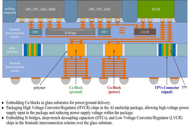
Cu blocks are used to replace TPVs/TGVs for power/ground delivery. This approach significantly reduces the number of TPVs/TGVs originally used for power/ground delivery through the glass substrate by 80%, thereby lowering fabrication complexity, improving manufacturing yield, and reducing manufacturing costs.
A current high-performance AI multichip package, comprising GPU chips and HBM modules, has more than 10,000 I/Os for power, ground, signal, and clock distribution, which requires more than 10,000 TGVs/TPVs in the glass substrate. 80% of these TGVs/TPVs in the glass substrate are used for power/ground delivery. Using Cu blocks to replace TPVs/TGVs for power/ground delivery results in an 80% reduction in the number of TPVs/TGVs, thereby lowering fabrication complexity, improving manufacturing yield, and reducing manufacturing costs. Nowadays high-performance semiconductor IC chips in AI multichip packages typically require more than 1,000 W of power. Since power (P) is given by P=I×V, a 1 V operation voltage of semiconductor IC chips corresponds to a current over 1,000 A.
As shown in Fig. 1, the embedded Cu blocks provide the power/ground voltage and current paths that would otherwise require a large number of TPVs or TGVs in the glass substrate. The remaining TPVs/TGVs (approximately 20%) are reserved for signal and clock transmission. Consequently, the embedded Cu blocks significantly reduce the number of TPVs/TGVs in the glass substrate.
The formation of embedded Cu blocks in glass substrates is achieved by inserting Cu blocks into pre-formed large holes in the glass substrate. This process is similar to the TPV Connector embedding process in glass substrates previously disclosed at SEMICON Taiwan 2025.
(2) Packaging Voltage Converter/Regulator (VCR) chips in AI Multichip Packages
The VCR chips are packaged vertically under and close to the GPU chip within the AI multichip package. The embedded VCR chips convert the 1,000 W, 48 V, 21 A power supply from external circuits to 1,000 W, 1 V, 1,000 A for the GPU chip. As shown in Fig. 1, copper blocks provide a low resistance power delivery system from external circuits to the embedded VCR chips, and resulting in reduction of the heat generation.
(3) Embedding Si Bridges, DTCs, and VCR chips in the Frontside Interconnection Scheme Over the Glass Substrate
At SEMICON Taiwan 2025, iCometrue® demonstrated that Si bridges and DTCs are embedded in large holes within the glass substrate. Here in Fig. 1, iCometrue® shows that Si bridges, DTCs, and VCR chips are instead embedded in the frontside interconnection scheme over the glass substrate, while the TPV connectors and copper blocks are embedded in large holes in the glass substrate. This approach further simplifies the fabrication of the AI multichip package using a glass substrate.
(4) Installing Electrical/Optical Connectors at the Edges of the AI Multichip Package
When glass substrates are used for multichip packaging, power and signals are usually input and output via the solder balls on the bottom of the multichip package through the backside interconnection (under the glass substrate), TPVs/TGVs (in the glass substrate), and the frontside interconnection (over the glass substrate) to the semiconductor chips. As discussed above, the fabrication of TPVs/TGVs is one of the major challenges in glass-substrate technology. To solve this problem, iCometrue® has introduced an innovative architecture that enables a large-size System-on-Panel (SOP) multichip package using a thick glass substrate without TPVs/TGVs.
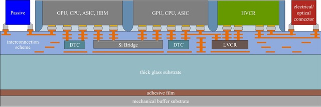
As shown in Fig. 2, power and signals are delivered through electrical and/or optical connectors located at the edges of the multichip package rather than through solder balls on the bottom of the package. The glass substrate is used as a panel-level fabrication platform and remains in the final package to provide mechanical support. An interconnection scheme (metal line and polymer) is built on the glass substrate, with electronic components such as interconnection bridges, integrated passive devices (IPDs), and VCR chips embedded within it. Semiconductor chips (CPU, GPU, ASIC, HBM) are then flip-chip bonded onto the interconnection scheme above the glass substrate. Electrical and/or optical connectors, together with passive components, are mounted on the top surface of the interconnection scheme using surface-mount technology (SMT).
Credit:iCometrue
Because power and signals are supplied by the edge connectors instead of bottom solder balls, signal transmission and power distribution from the edge connectors to semiconductor chips are through the interconnection scheme. Consequently, no TPVs or TGVs are required in the glass substrate, enabling large-size System-on-Panel (SOP) packages. Further, since no TPVs or TGVs are required, a thicker glass substrate can be used, which greatly reduces the bending of the glass panel. Thereby, the size of the glass panel used in the fabrication can be greatly increased.
More than Moore: The Use of Glass Substrates for Multichip Packaging
iCometrue® is pioneering a new era of advanced multichip packaging by introducing glass substrates with embedded TPV Connectors and Cu blocks, providing a practical and scalable alternative to conventional TGV-based processes. Further, embedding Si bridges, DTCs, and VCR chips in the frontside interconnection scheme over the glass substrate simplifies the fabrication of the AI multichip package. Combined with the TPV/TGV-free thick glass substrate architecture for System-on-Panel (SOP) packaging, these technologies establish a foundation for the next generation of multichip integration, extending Moore's Law into the era of glass-based system packaging and accelerating the advancem