The current growth cycle of the semiconductor industry is driven by the demand for logic and memory tied to artificial intelligence (AI), cloud infrastructure, and advanced electronics. This growth is expected to remain robust until 2026 and beyond. The Asia-Pacific region is one of the leading growth regions in this outlook.
However, this growth is increasingly constrained by interconnect economics and manufacturability, not just transistor scaling. As devices shift toward chiplets, memory-on-logic stacks, and high-density interposers, the package becomes a determinant of performance and cost.
In this context, hybrid copper bonding (Cu/oxide hybrid bonding) is transitioning from "advanced R&D" to a practical scaling solution because it enables high I/O density, reduced parasitics, and improved signal/power delivery pathways compared to solder microbumps. Additionally, it opens the door to lower-temperature integration for temperature-sensitive dies.
Hybrid bonding is not a niche process decision. It is a manufacturing capability decision that affects yield ramp speed and scrap risk, including interface integrity, voids, and consistency. It also affects cycle time and factory scheduling flexibility, including queue time stability and tool utilization. At the same time, it has implications for regional supply chain competitiveness, determining who can industrialize the technology at scale and replicate it across sites and regions.
Why Microbumps Become a Cost and Reliability Ceiling
Traditional solder microbump architectures introduce multiple interfaces and process steps that increase variability and cost. These architectures also face scaling limits in pitch, resistance, and long-term reliability as dimensions shrink.
Hybrid bonding addresses these constraints by combining dielectric-to-dielectric bonding with direct copper-to-copper connections, supporting pitches below 10 µm (with a trend toward lower pitches in leading use cases) while reducing interconnect length and parasitics. The result is lower latency and power.
Therefore, as pitch shrinks, the problem becomes less about "Can we bond?" and more about "Can we bond repeatably at high yield with acceptable thermal budgets across multiple factories and regions?"
The Manufacturing Sequence and the "Make-or-Break" Variable
A typical hybrid bonding flow begins with copper deposition using damascene or pillar-type electrochemical depositions, followed by CMP planarization for tight height and low roughness. Surface preparation, including oxide management and activation, is then performed before alignment and pre-bonding at near room temperature driven by dielectric adhesion. The process concludes with post-bond annealing, during which copper-to-copper diffusion and grain growth eliminate the interface.
While factors like orientation, surface cleanliness, and CMP are crucial, a key lever in the materials area becomes important because it directly impacts yield and schedule risks: the copper microstructure and surface morphology. These are strongly influenced by electrochemical deposition chemistry and govern atomic diffusivity, oxide disruption, and the grain growth necessary to eliminate the bonding interface.
Thus, if the copper's internal structure is "engineered" correctly, it can bond at lower temperatures while producing a robust, void-free interface, thereby reducing risk for advanced stacks and sensitive dies.
"Queue-Time Stability"
For high-volume manufacturing, newly plated copper must remain bond-ready despite real-world factory delays, such as metrology, transport, rework loops, tool availability, and cross-site logistics. Although freshly deposited copper is typically fine-grained, high-purity deposits can recrystallize quickly at room temperature, which can shrink the effective process window.
In comparative process evaluations, an ultra-high-purity copper process demonstrated visible surface grain growth within 2–4 hours after deposition and nearly complete recrystallization within 16 hours at room temperature. By contrast, a stabilized fine-grain approach maintained a largely unchanged microstructure across the same 2–16-hour window.
An optimized formulation can preserve this fine-grain structure for extended periods under ambient storage. It effectively decouples plating and bonding schedules and increases manufacturing flexibility.
Queue-time stability is a critical factory resilience feature. It reduces yield loss from "aging out" prior to bonding.
Microstructure Engineering with Everplate Cu 300 for Low-Temperature Cu-Cu Bonding
Everplate Cu 300 is an acidic copper electrolyte with the option to tailor it for a fine-grain copper approach with a dedicated additive package consisting of accelerator, suppressor, and leveler components. This system is designed to enable void-free feature filling while stabilizing a nanocrystalline microstructure against rapid recrystallization under ambient conditions.
Everplate Cu 300 FG is a process for depositing fine-grained, metastable copper. This material state supports direct Cu-to-Cu bonding and is particularly suited for advanced interconnect schemes, including low-temperature hybrid bonding in high-density integration environments.
The microstructural characterization results, based on SEM/FIB-SEM and EBSD analyses, connect process conditions to outcomes that directly impact manufacturability.
In terms of stability, fine-grain copper remains stable during multi-week ambient storage (reported to be >4 weeks) while retaining the ability to recrystallize upon thermal activation.
Regarding the process window around 200 °C, after extended room-temperature storage, a short pre-anneal (~10 minutes at ~200 °C) preserves the fine-grain structure. However, a longer thermal exposure (~2 hours at 200 ± 10 °C) drives substantial grain growth.
In terms of thermal margin without voids, annealing at an elevated temperature (e.g., 300 °C for several hours) does not necessarily result in void formation under controlled conditions.
In addition, in Cu/Cu/Ni multilayer stacks, prolonged exposure to moderate temperatures (e.g., 150 °C for 500 hours) can result in the disappearance of the Cu-Cu interface without detectable voiding. This indicates that the interface can be consumed within a practical thermal budget.
If a copper microstructure can remain stable for weeks and still "activate" during the bonding anneal process, then it can support better WIP scheduling flexibility, with less sensitivity to queue time; lower integration risk for temperature-sensitive stacks where the thermal budget must be constrained; and a higher probability of reproducible yields when scaling across sites and toolsets.
This is why microstructure engineering is more than just materials science. It is a route to repeatable, high-yield manufacturing.
The Broader Manufacturing Relevance
Rather than viewing hybrid bonding as a single "bonding step," it should be viewed as a chain of tightly coupled manufacturing windows: deposition, planarization, surface preparation, bonding, and post-bond thermal processing.
MKS's strategy is to address these types of problems with a systems-and-solutions approach. MKS' Atotech delivers process and manufacturing technologies across chemistry, equipment, software, and services. This is supported by a global TechCenter network and on-site customer support.
Scaling hybrid bonding is a cross-process optimization challenge. Vendors and manufacturers that can co-optimize adjacent steps, such as chemistry, equipment, process control, metrology, and logistics, will reduce time-to-yield and de-risk multi-site replication.
Asia's Evolving Semiconductor and Electronics Supply Chain
Not only is Asia's semiconductor supply chain expanding, it is also diversifying. Market projections point to continued global growth, with the Asia-Pacific region at the center of that trajectory. At the same time, regional activity reveals a clear shift toward capability, specialization, and technology leadership, rather than just scale.
Taiwan remains the focal point for next-generation semiconductor manufacturing, especially advanced packaging. The growing emphasis on hybrid bonding and fine-grained copper approaches highlights the push toward higher-density interconnects and tighter process integration at the wafer level.
Japan is reinforcing its role in the upstream part of the value chain, where materials, process development, and package substrate innovation converge.
Korea is increasingly treating advanced packaging as a strategic capability to extend its leadership in memory into higher-value AI-era integration, where HBM-driven 2.5D/3D architectures raise the bar on thermal management, warpage control, and interconnect density. Policy support is reinforcing this direction through a multi-year, state-backed packaging R&D program and broader semiconductor ecosystem measures aimed at strengthening domestic back-end and supply-chain competitiveness.
Further south, Southeast Asia is moving forward in its role as a volume manufacturing base. New facilities and accelerated roadmaps indicate a starting gradual shift toward more advanced process steps and higher value contribution. Meanwhile, India is emerging as a developing ecosystem with a growing focus on building domestic semiconductor and advanced packaging capabilities.
The result is a more distributed and specialized supply chain. Taiwan is leading the way in scaling up advanced manufacturing, Korea extending its leadership, Japan is anchoring process and materials innovation, Southeast Asia is expanding its capability footprint, and India is positioning itself for long-term ecosystem growth. Together, these shifts point to a regional model that is defined less by cost arbitrage and more by technological differentiation and supply chain resilience.
Redefining Readiness for Hybrid Bonding
Senior decision-makers must adjust not just their priorities, but also how they define readiness. Hybrid bonding is no longer just a research milestone; it is now an operational key performance indicator (KPI). Queue time limits, CMP variability, bond yield, and thermal budget margin are direct indicators of manufacturing performance.
The competitive shift is equally clear: process window robustness matters more than peak performance. The ability to maintain stable microstructures over time and activate them reliably under tightly controlled thermal conditions is becoming the defining factor for scale.
This elevates co-optimization from a best practice to a requirement. Advantage increasingly lies in the integration of chemistry, equipment, process control, and via formation to deliver consistent interconnect outcomes, rather than in any single process step.
The implication is strategic and immediate: success will depend on the ability to industrialize advanced packaging within narrowing process windows across multiple geographies without losing control.
Hybrid Bonding as a Competitive Manufacturing Capability
Hybrid copper bonding is emerging as a cornerstone interconnect technology for fine-pitch 2.5D and 3D integration. However, its adoption is not solely defined by feasibility, but also by the ability to consistently deliver void-free, low-resistance Cu-Cu interfaces within increasingly constrained thermal budgets.
A growing body of evidence from the manufacturing process indicates that engineering metastable, fine-grain copper yields a combination of characteristics that are operationally decisive: extended queue-time stability paired with rapid, thermally activated grain growth. This supports interface elimination without void formation under controlled conditions.
Scaling these capabilities is inseparable from ecosystem integration. It depends on how effectively process chemistry, equipment, software, services, and adjacent manufacturing steps are combined into a unified interconnect strategy.
This integration is crucially being driven in regions where electronics manufacturing is advancing most rapidly, particularly across Asia. Consequently, the ability to replicate tightly controlled processes across multiple sites is becoming a defining requirement.
The implication is clear: as advanced packaging scales globally, competitive advantage will accrue to those who can translate microstructural control into production-level consistency across tools, processes, and regions. In this context, hybrid bonding is not only a technological turning point, but also a test of manufacturing maturity.
For more information about this article and whitepaper, please click the link.
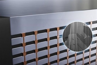
Fine-grain copper for reliable hybrid bonding. Credit: MKS-Atotech
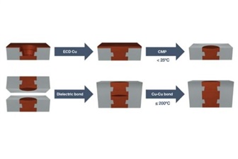
Hybrid bonding sequence: Cu fill, CMP, pre-bond, annealing. Credit: MKS-Atotech