

Applied Materials aims to begin work on its proposed 140-acre semiconductor research campus in Bengaluru in 2027, marking the first phase of a US$5 billion investment program that significantly expands the company's earlier plans for equipment development in India.
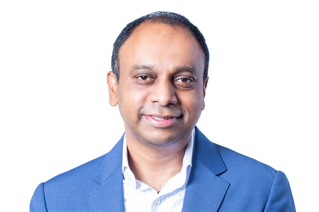
Avi Avula, president and managing director of Applied Materials India, told DIGITIMES that the new project incorporates the US$400 million engineering center announced in 2023, but extends its scope beyond supplier development to include complete semiconductor equipment product development for global customers.
The first phase will take at least two to three years from groundbreaking to become operational, with subsequent expansion dependent on internal approvals and the pace of development.
The company is also seeking to establish a supplier ecosystem around the research campus, bringing international equipment component manufacturers and Indian companies closer to its R&D operations.
Earlier investment incorporated into larger expansion
The new investment program represents a shift from Applied Materials' original plan to establish an engineering center focused primarily on components, subsystems and supplier development.
Avula said the company reassessed its strategy over the past 18 to 24 months, deciding to pursue a broader role in semiconductor equipment development rather than limiting its Indian operations to supporting manufacturing activities elsewhere.
The US$400 million commitment is now included in the US$5 billion program, rather than being treated as a separate investment.
"We blended that into this 5 billion, but that lab ... is much larger than the 400 million," Avula said.
Applied had acquired 10 acres for the earlier project but now intends to sell that property and consolidate its development activities at the proposed 140-acre campus near Bengaluru airport.
The land transfer for the new site is nearing completion, Avula said, adding that the Karnataka government had facilitated the process.
Applied expects to begin some activity at the site in 2027 after submitting its proposals under the India Semiconductor Mission policy framework. However, each development phase will require internal board approval.
The company has not disclosed how it will allocate the US$5 billion across different activities, as spending will depend on the scale and timing of successive phases.
Avula said a substantial portion would go towards R&D infrastructure, including laboratories resembling a smaller semiconductor fabrication facility, alongside investment in engineering and research personnel.
Unlike commercial fabs, the proposed facilities will focus on developing, testing and validating semiconductor manufacturing equipment rather than producing chips.
India to assume greater responsibility for equipment products
The expansion is intended to transform Applied Materials' India operations from a predominantly engineering support organization into a business with direct responsibility for semiconductor equipment products and revenue.
Avula said the company's 25-year presence in India had largely involved providing engineering and other services to its global headquarters. The next stage will involve developing products locally for semiconductor manufacturers worldwide.
Applied plans to give Indian teams end-to-end responsibility for selected equipment product lines, covering design, development, manufacturing, validation, marketing, sales, and customer engagement.
The initial focus will be on what the company describes as "trailing edge" products, while the most advanced equipment development will continue to be led from the US.
Avula stressed that trailing-edge equipment remains technologically sophisticated and is used in advanced semiconductor fabs. Indian engineers also continue to contribute to the company's leading-edge technologies and customers.
"What is the distinction here is we're going to own everything for the trailing edge," he said.
The transition builds on work already underway at Applied's India Validation Center in Bengaluru, which houses 10 process tools for 300mm wafer processing.
Avula said the facility has demonstrated the ability of Indian teams to develop equipment products and engage directly with customers. Products developed and built in India have already reached semiconductor fabs overseas, with further deployments expected.
The larger campus is intended to extend those capabilities across more product lines, allowing the India operation to assume responsibilities resembling those of an independent business unit within Applied Materials.
Local suppliers key to equipment development
Developing a local supplier base will be critical to the expansion, particularly as equipment products developed in India remain heavily dependent on imported components and technologies.
Avula said more than 90% of the build for products developed locally has come from overseas, with equipment, subsystems and other technologies sourced from countries including Japan, the US and locations in Southeast Asia.
Applied intends to expand its India-based supply chain tenfold, although Avula acknowledged that the increase would come from a relatively small existing procurement base.
A majority of its current suppliers in India are domestic companies, while a smaller number are international manufacturers with local operations. Several already supply components to Applied's manufacturing facilities in Singapore and the US.
The company is seeking to expand this network by working with Indian manufacturers serving industries such as automotive and aerospace, where some existing capabilities could be adapted to semiconductor equipment requirements.
However, advanced ceramic components, radio-frequency technologies and vacuum systems remain difficult to source locally because of their technical complexity and the specialized manufacturing capabilities required.
Avula said the company would initially focus on components where Indian manufacturers face smaller technology gaps, while working over time to qualify more sophisticated subsystems.
The proposed research campus is expected to accelerate that process by allowing suppliers to test components directly in Applied's equipment under conditions comparable to those in semiconductor fabs.
Currently, components developed in India often need to be shipped to Applied's laboratories overseas for evaluation, increasing development time.
"We can't wait for the ecosystem to develop on its own," Avula said.
Applied is in discussions with dozens of Indian and international companies about potential collaboration, including opportunities to establish operations alongside its proposed R&D facilities.
The company also hopes the investment will encourage established international suppliers to consider India when deciding where to build new manufacturing capacity.
Higher-value localization to determine progress
While expanding domestic sourcing is a priority, Avula said the value and technical complexity of locally manufactured components would be more important measures of progress than their share of overall procurement.
Simpler components offer relatively limited opportunities for differentiation, while advanced subsystems could enable Indian suppliers to develop specialized expertise and intellectual property.
"It's less about the percentage of what is local versus the value components that are local," he said.
Developing these capabilities would also provide opportunities beyond Applied Materials, as qualified suppliers could potentially serve other semiconductor manufacturers establishing operations in India.
For Applied, the longer-term objective is to increase both the number of equipment products developed in India and the contribution of domestic suppliers to their manufacture.
The pace of that transition will depend in part on bringing the first R&D facilities into operation, giving Indian companies access to the testing infrastructure needed to qualify increasingly complex equipment components.
Article edited by Jack Wu