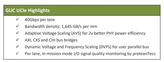
Global Unichip Corp. (GUC), the Advanced ASICLeader, announced today that it has successfully taped out Universal Chiplet Interconnect Express (UCIe) PHY IP with 40Gbps per lane on TSMC's N5 process, beyond UCIe's highest speed, for AI/HPC/xPU/Networking applications. UCIe 40G chiplet interface provides an industry-leading bandwidth density of 1,645 GB/s per mm of die edge. The IP supports any speed up to 40Gbps and uses Adaptive Voltage Scaling (AVS) to reduce supply voltage achieving 2x better power efficiency for required speed. The chip is assembled using TSMC's CoWoS (Chip on Wafer on Substrate) advanced packaging technology.
Following suit GUC's world first UCIe 32G solution readiness on TSMC's N3P process in the industry in 2023, GUC further taped out UCIe 40G on the TSMC N5 process for meeting high bandwidth demand of multi-die integration at AI/HP/Networking applications. To further reduce PHY power, GUC features Adaptive Voltage Scaling (AVS), to optimize PHY supply voltage and driving strength, improving power efficiency by 2x. Minimal supply voltage and driving strength are selected by training algorithm to meet eye-opening margins criteria ensuring robust operation in changing voltage and temperature conditions. The IP integrates silicon-proven proteanTecs' I/O signal quality monitors. Signal quality is monitored in mission mode, during data transfer, without re-training or causing any data transfer interruption.
For easy integration, GUC developed bridges for AXI, CXS, and CHI buses using UCIe Streaming Protocol. These bridges are optimized for high traffic density, low power, low data transfer latency, and efficient end-to-end flow control, facilitating a seamless transition from single-chip NoC to chiplets architecture. The bridges support Dynamic Voltage and Frequency Scaling (DVFS) allowing digital supply voltage and bus frequency change on the fly while ensuring uninterrupted data flow. To support the IP integration in the bottom dies using TSMC's SoICR-X technology, it can be placed "face up" by adding TSVs for supplies and interface signals.
"We are thrilled to announce our new-generation UCIe IP supporting 40 Gbps with 2x better power efficiency," said Aditya Raina, CMO of GUC. "We have established a complete silicon-proven 2.5D/3D chiplet IP portfolio at TSMC's 7nm, 5nm, and 3nm technologies. Together with design expertise, package design, electrical and thermal simulations, DFT, and production testing for the TSMC 3DFabricRofferings including CoWoSR, InFO, and TSMC-SoICR, we provide our customers with a robust and comprehensive solution, enabling fast design cycles and quick bring up of their AI/HPC/xPU/Networking products."
"We are committed to delivering the fastest and the lowest power 2.5D/3D chiplets interface IPs, facilitating a seamless transition from monolithic to chiplets architectures," said Igor Elkanovich, CTO of GUC. "Convergence of 2.5D and 3D packaging using HBM3/4, UCIe and GLink-3D interfaces enables highly modular, much bigger than reticle size processors of the future."

Credit: GUC


