


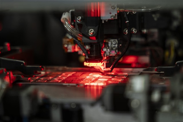
India's effort to modernize its state-run Semiconductor Laboratory (SCL) is shaping up to be one of the most consequential experiments in the country's semiconductor strategy.
The government is spending INR4,500 crore (US$505 million) to upgrade the Mohali facility's 200-millimeter line, aiming to shift it from a legacy research unit into a source of mature-node chips for automotive, industrial, and defense applications.
Unlike private fabs that dominate global chipmaking, the upgraded facility will remain fully government-operated. That design choice is drawing a mix of optimism, caution, and structural warnings from semiconductor analysts.
India's bet on a state-operated fab
Some experts see the move as a strategic statement. Danish Faruqui, CEO of Fab Economics, a greenfield fab/ATP projects advisory consultancy, calls the upgrade an "unprecedented role modeling exercise," arguing that India is attempting what few countries have tried: operating a modern fab inside the public sector for both strategic and limited commercial output.
Faruqui says a government-run source of essential chips could offer India the supply assurance that the US and Europe still depend on private foundries to secure.
"This is a role modeling project for the Government of India to show the world that fabs can be operated by governments," Faruqui said. "Since this is a strategic segment and every government is prioritizing semiconductor capability, India will showcase in an unprecedented way that a captive fab for government and commercial purposes can be run by the state."
Sanchit Vir Gogia, chief analyst at Greyhound Research, agrees the investment gives SCL a platform to reinvent itself, provided the operating environment becomes more agile. Faster decisions, clearer norms, and consistent engineering support could help the fab stabilize yields, he said.
But others see limits to how far a state facility can push commercial performance. Manish Rawat of TechInsights warns that even private fabs struggle to ramp yields quickly.
"Running a 200-millimeter fab efficiently is challenging even for experienced private-sector teams," Rawat said. "Government-operated fabs globally have struggled to reach commercial-grade yields because they move more slowly on process deviations and optimization cycles. Without incentives and strong accountability, yield improvement could take several quarters or even years."
Coordination risks rise inside a three-vendor structure
India has divided the modernization into three packages spanning equipment, design enablement, and automation. The model gives India access to multiple capabilities, but analysts say it also places unusual demands on coordination.
Gogia believes the structure can work if a central technical authority is empowered to align tool bring-up, process recipes, and automation across vendors. Without that, he says, the effort risks becoming disjointed.
Rawat is more direct, warning of a potential "blame loop" if yields fall short. Faruqui goes further, noting that the current structure does not resemble standard semiconductor execution models. He says fabs typically rely on integrated program, platform, and product teams that track tool efficiency, MPW schedules, reliability metrics, and site-level KPIs. He recommends that India appoint a domain-specific program management consultancy with clear performance indicators monitored by the government.
A talent lift that could cut both ways
The upgrade is expected to produce a wave of newly trained engineers familiar with advanced tools and processes. That capability could strengthen India's broader semiconductor workforce, but analysts say the benefit may not stay within SCL.
Rawat cautions that the lab could become a taxpayer-funded upskilling pipeline for private fabs unless retention incentives improve. Gogia believes SCL can hold talent if roles offer technical depth and a sense of mission.
"Institutions tend to retain skilled engineers when the work offers depth, a sense of mission, and long-term growth," Gogia said. "SCL has the opportunity to provide exactly that by creating specialist roles and exposure to strategic programs."
Faruqui suggests more formal mechanisms.
"There has to be a timeline commitment by newly trained engineers to ensure that taxpayer-funded training turns into capacity building rather than a training ground for private fabs," Faruqui said. "Training must proliferate across operations, R&D, and technology development at speeds aligned with semiconductor methodology."
Fragmented customer experience could slow startups
The design-to-fab flow is another area where analysts see risk. Cyient will support design enablement, while SCL will handle fabrication. For experienced chip designers, this may be manageable. For startups, it may be difficult.
Gogia says a single-window interface would prevent customers from navigating boundaries between vendors. Rawat warns that unclear ownership of tape-out failures could stall early-stage development.
Faruqui identifies a deeper gap: the lack of a productization function. Large chip companies rely on teams that track wafer data layer by layer. Startups cannot build these teams, so he suggests the government consider offering a domestic, shared productization unit to support early customers.
Procurement bottlenecks remain a central risk
Fast maintenance cycles define semiconductor manufacturing, but India's procurement system remains slow and rule-bound. Analysts say that unless procurement authority is delegated, the new tools risk falling short of their potential.
Gogia and Rawat both recommend fast-track budgets and long-term service contracts.
Faruqui adds that SCL needs a formal production planning and control organization with operational autonomy to manage wafer starts, lot scheduling, and equipment efficiency in real time. Without this, he says, maintenance and throughput would remain vulnerable.
A strategic facility more than a volume engine
Even with the upgrade, analysts do not expect SCL to become a high-volume commercial foundry. Instead, they see different measures of success.
Gogia believes SCL can anchor India's OSAT ecosystem by supplying trusted mature-node wafers. Rawat expects the fab to operate as a prototype and specialty-node facility unless structural reforms accelerate. Faruqui argues that sovereign supply of essential chips is the real metric and calls the project a strategic move if governance is strong.
The SCL modernization will test far more than equipment installations or new process technologies. It will reveal whether India's public sector can manage the speed, integration, and autonomy required to run a modern semiconductor facility.
The result will shape how global chipmakers assess India's execution capabilities and may influence how other governments think about their own approaches to securing semiconductor capacity.
Article edited by Jerry Chen