CONNECT WITH US

Interview: Andhra Pradesh moves to become India's semiconductor packaging hub

, DIGITIMES Asia, Taipei
0

Credit: DIGITIMES

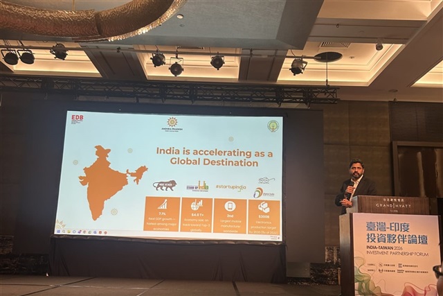
Andhra Pradesh is making its most concrete move yet in semiconductors, zeroing in on packaging as the immediate entry point into the chip supply chain. Speaking on the sidelines of the Computex technology expo in Taipei, Bhaskar Katamneni, Secretary to the Government for ITE&C, acknowledged that wafer fabrication remains a long-term "seven or eight-year journey," but said packaging work is already well underway — with four PCB manufacturers having already begun operations, according to him.

ASIP leads the charge

Leading that push is Advanced System in Package (ASIP) Technologies, which is set to break ground on the state's first commercial-scale OSAT and assembly, testing, marking, and packaging (ATMP) facility on June 8 — a date confirmed by Katamneni in an interview. According to previous reporting by DIGITIMES Asia, ASIP and South Korea's APACT Co. Ltd. began pursuing the project in 2024, positioning the facility as part of India's broader effort to establish domestic semiconductor packaging and testing capacity and integrate into global semiconductor supply chains.

Approved under India's central government Semiconductor Mission (ISM), the plant in Tarluvada, Visakhapatnam, is designed to produce 96 million chip units per year, with an initial investment of INR468 crore (US$48.95 million) and long-term phase-wise scaling projected to reach up to INR2,387 crore. Specializing in Flip Chip Ball Grid Array (FCBGA) and Wire Bond Quad Flat No-Lead (QFN) integrated circuits, the facility will target smartphones, automotive electronics, and consumer devices.

Credit: ASIP

Credit: ASIP

PCB momentum builds

The pipeline extends further still. As previously reported by Tele.net magazine, Syrma SGS Technology, through its subsidiary Syrma Strategic Electronics, is building what has been described as India's largest PCB manufacturing facility near Naidupeta in Tirupati district. The project encompasses multilayer, HDI, and flexible PCB production, alongside a copper-clad laminate (CCL) facility and electronics manufacturing services (EMS) operations. Construction began in late 2025, with trial production targeted for 2026-27.

Wooing Taiwan

The semiconductor push coincides with an active diplomatic and investment drive at Computex, where Katamneni said senior officials have identified at least four to five Taiwanese companies expected to break ground on new facilities within the next four months. The state's delegation is using the trip to solidify joint ventures and direct investments in electronics, semiconductors, and PCB manufacturing. By the time Computex comes around next year, the state anticipates many of these units will have already commenced factory construction.

A 6.5 GW data center ambition

Beyond chips, the state's strategy centers on a massive expansion of AI data center infrastructure, with a target of 6.5 gigawatts (GW) in capacity over the next five to six years. Katamneni highlighted a recent announcement by Google for a 1 GW hyperscale data center as a cornerstone of this initiative. These centers are primarily being clustered in Vizag, where the state is developing an ecosystem of 30 to 40 large units, each occupying between 500 and 1,000 acres.

"My province is very specifically well-suited to data centers because we are on the coast," Katamneni said, noting that undersea cables are being connected to Singapore to provide high-speed global connectivity. To manage the environmental impact, the state plans to run these facilities on 100% renewable energy — utilizing surplus solar and wind — and intends to use water diverted just before it reaches the sea for cooling purposes.

Under the microscope

However, the planned hyperscale AI data center cluster in Visakhapatnam has also drawn scrutiny over its environmental footprint. In an opinion piece published by The Hindu, the project was described as a major challenge for Andhra Pradesh, with the author arguing that policymakers have focused heavily on investment and technology ambitions while paying insufficient attention to the infrastructure demands required to support such facilities.

The article noted that hyperscale AI data centers consume vast amounts of electricity and water, raising questions about the long-term sustainability of hosting projects of this scale in a region already facing resource constraints.

Built to cluster

The state's hardware ambitions extend beyond individual facilities to the creation of co-located industrial clusters. Katamneni noted that the government is designating specific locations for memory chips and battery manufacturing to complement its existing PCB and packaging hubs — an approach intended to build a comprehensive hardware ecosystem where different verticals, from design teams to final assembly, operate in proximity to maximize efficiency.

Geography reinforces that logic. Situated between the design-heavy hub of Bangalore and the manufacturing center of Chennai, Andhra Pradesh aims to position itself as a "common market" offering cheap land, water, and power, backed by a workforce of 200,000 new engineers annually. By streamlining these sectors within a single state, the government is looking to leverage India's common market status — allowing components to be fabricated, packaged, and integrated into final products across the country without the cross-state tax barriers that historically hindered domestic supply chains.

"We take advantage of the design capabilities of Bangalore and the manufacturing capabilities of Chennai," Katamneni said.

Governing smarter

The push for hardware is mirrored by internal digital transformations. The state's "Real Time Governance" initiative uses AI to move from reactive to proactive service delivery. By digitizing workflows, the government has eliminated paper, using AI tools to summarize files and suggest policy solutions, which Katamneni says allows officials to focus on execution rather than paperwork.

Article edited by Jack Wu