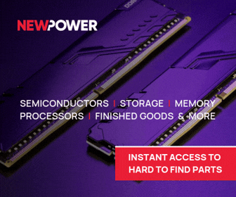
SK hynix announced today that it has begun supplying its high-performance mobile NAND solution ZUFS 4.1 to customers, marking the world’s first mass production of this solution.The solution's adoption in the latest smartphones reinforces SK hynix's technological excellence in the global market. ZUFS 4.1 will enhance smartphones’ powerful on-device AI capabilities, offering users an innovative experience.SK hynix successfully completed the qualification process for the solution in June this year through close collaboration with customers. In July, the company began mass production and started supplying the product.ZUFS, or Zoned UFS, is an extended specification of UFS that applies Zoned Storage technology, which stores data in different zones based on its usage and characteristics.When installed in a smartphone, ZUFS 4.1 enhances the operation speed of the operating system (OS) and improves data management efficiency. As a result, it mitigates read performance degradation over extended use by more than four times compared to conventional UFS, enabling a 45% reduction in app launch times. Unlike conventional UFS, which writes new data by overwriting existing data, ZUFS 4.1 writes data sequentially. This data storage method has resulted in a 47% reduction in AI app launch times.These performance characteristics position ZUFS 4.1 as an optimal solution for today's mobile environment, where on-device AI and large-scale data processing are essential.In addition, SK hynix has significantly enhanced the error-handling capabilities of ZUFS 4.1 compared to version 4.0 developed in May 2024. By detecting errors with greater precision and clearly communicating the necessary corrective actions to the central processing unit, the latest solution is expected to significantly improve system reliability and recovery performance.“ZUFS 4.1, which we have successfully begun to supply, is the first solution developed and mass-produced through collaboration aimed at optimizing Android OS and storage devices. Looking ahead, its applications are expected to expand,” said Justin Kim, President & Head of AI Infra at SK hynix.“We will continue to supply NAND solutions that meet customer needs in a timely manner, while strengthening partnerships with global companies to strengthen our competitive edge in the AI memory sector.”Credit: SK Hynix
As digital infrastructure becomes the backbone of today's enterprises and cloud services, servers have transformed far beyond their original role as mere computing units. They now function as central nodes for computation, storage, and connectivity. Within this transformation, Flash Memory has assumed a much more critical role. No longer a passive storage medium for firmware, Flash Memory today underpins server security, trust establishment, and operational resilience.In a modern server, essential functions such as secure boot, firmware updates, identity credentials, encryption keys, and audit logs all rely on Flash Memory. This convergence of code and data means that any compromise of Flash Memory can have catastrophic consequences, potentially granting attackers control over the entire IT infrastructure. For adversaries, targeting the operating system is no longer necessary; infiltrating firmware embedded in Flash Memory can yield far more persistent and devastating results. Once the root of trust is undermined, neither the operating system nor the application layer can be fully trusted, regardless of the protections in place.The Shifting Threat Landscape: From OS to FirmwareIn recent years, multiple real-world incidents have revealed a concerning trend: attacks are no longer confined to software or network vulnerabilities but are reaching deep into firmware and memory. For instance, a compromised Baseboard Management Controller (BMC) firmware can create stealthy, persistent threats invisible to the operating system. Similarly, supply chain attacks have introduced malicious code during the manufacturing or update process, leaving organizations vulnerable even before deployment.Unsecured memory interfaces have also been exploited to execute unauthorized code within servers, effectively bypassing authentication safeguards. The common denominator in these attacks is clear: adversaries are bypassing traditional software defenses and striking directly at the hardware foundation. This makes firmware security—and by extension, Flash Memory security—the new frontline of cyber defense.To learn the latest cybersecurity regulations and trends, download the hardware security whitepaper for free.From Passive Storage to Active Security EnablerTraditionally, Flash Memory was seen as a passive storage component—responsible only for reliable read and write operations. That paradigm no longer holds. In the face of increasingly sophisticated attacks, Flash Memory must evolve into an active participant in security enforcement.Modern servers now demand that Flash Memory deliver capabilities well beyond performance and density. At the hardware level, access control must prevent unauthorized read and write attempts. Firmware execution or updates must be validated before they can occur, while rollback prevention ensures that attackers cannot revert the system to older, vulnerable versions.Flash Memory also has to serve as a secure vault for encryption keys, including those designed for post-quantum cryptography (PQC). At the same time, it must provide tamper-evidence, event logging, and auditing support—crucial for forensic analysis. Equally important, Flash Memory must integrate with secure supply chain verification and digital signature validation, ensuring that every firmware image comes from a trusted source.These requirements are not optional. They reflect compliance with internationally recognized security standards. The U.S. NIST SP 800-193 defines resilience requirements for platform firmware. UEFI Secure Boot has become a baseline mechanism to safeguard startup integrity. Meanwhile, frameworks such as NIST 800-161 and the EU Cyber Resilience Act address risks tied to globalized supply chains. Collectively, these standards also lay the foundation for a post-quantum security landscape, where digital signatures must remain resistant to future quantum attacks.Winbond W77Q: Securing the Future of Servers In response to these growing challenges, Winbond has introduced the W77Q secure Flash Memory series, delivering a trusted solution for modern server design. Unlike conventional flash, W77Q integrates security logic directly into the memory device, transforming it from a passive component into an active enabler of system defense.One of the defining features of W77Q is its comprehensive support for secure boot. By embedding digital signature verification, W77Q ensures that servers begin execution in a trusted state from the very first instruction. The device even supports LMS-based algorithms—designed to withstand quantum-era threats—providing forward-looking assurance against tomorrow's risks.Equally important is the secure handling of cryptographic keys. W77Q can isolate keys within a hardware-protected zone, including PQC-compatible keys, shielding them from system-level vulnerabilities or external exploits. Every attempt to modify firmware must pass a hardware validation process, effectively blocking malicious injections before they take hold.W77Q's integrated cryptographic engine supports advanced digital signatures, verifying firmware authenticity directly within the flash device. Whether firmware is preloaded during manufacturing or delivered later through updates, W77Q independently validates its origin and integrity, reducing reliance on host processors and closing off critical attack vectors.By embedding security into the memory layer, W77Q mitigates several high-risk scenarios: firmware hijacking during production, tampering during logistics, insertion of fake updates through compromised channels, and unauthorized modifications that bypass operating system checks. This memory-centric defense ensures protection across the server's entire lifecycle, from factory floor to deployment and beyond.Supply Chain Integrity in the Post-Quantum EraThe rise of outsourced manufacturing and globally distributed supply chains has amplified the complexity of server security. Cybersecurity is no longer the responsibility of individual enterprises alone but a shared obligation across every participant in the supply chain. A vulnerability at any stage—from fabrication to firmware distribution—can be weaponized by attackers to infiltrate the end product.In this environment, memory-level verification becomes not just a best practice but an essential requirement. Secure flash that supports both PQC and supply chain validation ensures that every stage of the process remains verifiable and trustworthy. W77Q embodies this principle, equipping server manufacturers with a solution tailored to the challenges of globalization and quantum-era security.Building the Next Generation of TrustThe evolution of Flash Memory from passive storage to a root of hardware trust reflects a broader industry realization: security must be enforced at every layer, starting from silicon and extending all the way to the cloud. As servers form the backbone of digital society—supporting everything from financial systems and healthcare to AI model training and deployment—the integrity of these platforms is non-negotiable.By launching the W77Q secure flash series, Winbond is not only addressing today's server security requirements but also laying groundwork for the future. With support for PQC, supply chain validation, and zero-trust architectures, W77Q empowers server manufacturers to construct resilient defenses against an increasingly dynamic threat landscape.In a world where trust is both a guarantee of reputation and a prime target for attacks, securing memory at the foundational level means securing far more than a single product. It represents safeguarding entire business models, digital ecosystems, and the trust of millions of users. Flash Memory, once a silent storage element, has now emerged as the first line of defense for the digital future.To learn more about Winbond's advanced security solutions, visit Winbond's website or contact Winbond directly, or download the latest Hardware Security White Paper.
Taiwan-based advanced packaging equipment provider C SUN Manufacturing, Ltd. (TWSE: 2467), now in its 60th year, is undergoing a critical transformation as it expands from its roots in PCB and thermal processing equipment into the forefront of semiconductor advanced packaging. Founded in 1966, C SUN has evolved into a key supplier across the AI semiconductor value chain. Through G2C+ Alliance, the company has established strategic sites across Linkou, Hsinchu, and Taichung: Taiwan's west coast "Golden Corridor" to provide localized support for foundry and OSAT customers.As AI technology progresses through four key stages: perception, generation, reasoning, and physical execution, advanced packaging has become essential for sustaining Moore's Law. Industry analysts point to aggressive capacity expansion from TSMC between 2022 and 2026, with annual growth rates projected at 80% for AI testing and CoWoS, and 100% for SoIC technologies. This surge presents a significant opportunity for equipment suppliers who can keep pace with evolving process requirements.C SUN began co-developing advanced packaging equipment with global semiconductor leaders in 2012. Since then, precision demands have grown exponentially. In the first half of 2025, advanced packaging equipment already contributed 40% of C SUN's revenue, a tenfold increase over the past five years.Building on its legacy as a leader in PCB equipment, the company is also capitalizing on the evolution of HDI for AI technologies. It supplies critical process tools such as desmear, PTH, lamination, and debonding. PCB-related sales accounted for 51% of revenue in the first half of 2025, with advanced PCB revenue alone growing 7x in the past five years. To support these dual growth engines, C SUN has preemptively expanded its engineering workforce by 30% over the past three years, laying the foundation for its next decade.In H1 2025, C SUN reported NT$2.819 billion in revenue, marking a 16.1% year-over-year increase. Notably, equipment sold into the AI industry chain accounted for over 65% of total sales. The two primary growth drivers: advanced packaging and advanced PCB, remain at the center of C SUN's strategic focus. Moving forward, the company will continue to expand its AI-related portfolio, not only CoWoS, but also WMCM, SoIC, HBM, burn-in test, IC substrates, and advanced HDI. The roadmap further extends into emerging sectors such as reclaimed wafers and glass substrates.From a macro perspective, C SUN is uniquely positioned to benefit from the convergence and diversification of AI hardware ecosystems. As the boundaries between foundry and OSAT operations blur under the emerging “Foundry 2.0” model, and as AI-specific demand rises in the PCB sector, equipment suppliers are entering their golden age. Since 2024, OSATs have taken on more outsourced work, opening new collaborative opportunities for toolmakers.C SUN has already seen success with the adoption of its vacuum pressure ovens in OSAT processes and is expanding into CoW-level applications. As demand for high-performance computing (HPC) chips grows, the company is scaling up with top global OSATs, including overseas deployments. Though this expansion entails near-term costs, C SUN expects strong long-term revenue contributions given the high value of its equipment portfolio.Looking ahead, C SUN stands out as one of Taiwan’s few players with deep involvement in both advanced PCB and semiconductor packaging. It plays a pivotal role in the upstream AI server supply chain. With major US-based CSPs continuing to increase capex, C SUN is positioning itself as a core enabler of the global AI packaging wave, ready to ride the next high-growth cycle.Credit: Company
In the wake of the AI and Electric Vehicle (EV) era, efficient power supply and conversion have become a critical battleground. For over a decade, 3S Silicon Tech has been deeply committed to developing high-reliability packaging equipment for power devices and modules. Over the past five years, the company's formic acid vacuum reflow oven has gained widespread acclaim from leading international IDMs and the world's largest OSATs. Its remarkable advantages—including low void rates, flux-free soldering, and post-solder cleaning-free processes—effectively resolve metal oxidation issues, establishing 3S as a leading brand for high-end power module reflow packaging.From data to prediction: AI empowers equipment3S Silicon Tech's core technology utilizes AI to build process behavior models, enabling equipment to learn from data, predict, and self-optimize. Through machine learning (ML), the system analyzes vast amounts of data from sources like MES, sales, and SQL databases to identify key process variables.This allows the equipment to learn from past experience and provide precise parameter recommendations, leading to:1. Precise process tuning: The AI model recommends optimal parameters for different product types, ensuring perfect soldering every time. For example, baseline models for heating elements in various temperature zones are established before the equipment leaves the factory. By continuously monitoring the heating elements, the AI uses predictive analysis to issue early warnings before a malfunction occurs, ensuring process stability, preventing unexpected downtime, and even predicting the lifespan of the heating element.2. Yield and quality optimization: AI analysis quantifies the interactive relationships between different parameters and variables. Using a correlation matrix model, it provides optimal parameter recommendations for power modules, effectively boosting yield and product reliability.3. Precise predictive profiling: This technology effectively prevents up to 99.99% of equipment failures, optimizing production efficiency, reducing downtime, and significantly lowering maintenance costs.Green sustainability: Achieving flux-free solderingBeyond intelligence, this new launch also emphasizes sustainability. 3S Silicon Tech's AI-empowered formic acid vacuum reflow oven features a unique flux-free soldering capability. This not only enables a clean and highly reliable soldering process without the need for post-solder cleaning, but also reduces waste by up to 99%, providing a dual benefit of environmental protection and cost control for businesses.3S Silicon Tech sincerely invites you to SEMICON Taiwan 20253S Silicon Tech's AI-empowered formic acid reflow oven offers semiconductor manufacturers a highly efficient and easily implementable solution. This technology is specifically designed to address customers' void rate concerns, clearly demonstrating the immense application value of AI in semiconductor manufacturing. It further helps companies achieve a comprehensive upgrade in yield stability, predictive analysis, and maintenance optimization.3S Silicon Tech cordially invites all industry professionals and partners to visit our Booth Q5338 at Hall 2 of the Nangang Exhibition Center during SEMICON Taiwan from September 10-12, 2025. Come experience our cutting-edge AI and formic acid reflow oven technology and witness the journey toward smart, optimized manufacturing. For more information, please visit the 3S Silicon Tech Official Website.
The age of AI greatly boosts Semiconductor manufacturing demands in advanced packaging. As packaging complexity increases (more I/O, smaller bump pitches, higher density), making the integration of nano-precision platforms and thermal stabilization in Semiconductor automation a strategic investment.PBA Systems will debut its latest nano-precision dual gantry platform series and metrology stage series designed for CoWoS and smart manufacturing requirements, to be showcased in the 2025 SEMICON Taiwan exhibition, located at Hall 2, 1st floor, Booth Q5536 in the Taipei Nangang Exhibition Center from Sep. 10th to Sep. 12th.For semiconductor advanced packaging technologyThe technology drivers of Heterogeneous Integration Architectures in Semiconductor advanced packaging involve different materials and bump density, and drive different process equipment requirements. From 2.5D to 3D development, semiconductor advanced Packaging may require different Die Attachment Processes, from high-speed, high-accuracy to thermal compressed and hybrid bonding. These processes require highly precise, custom-designed platforms for automation.PBA's latest dual gantry nano precision platform series offers high precision solutions for flip-chip bonding, thermo-compression bonding, and hybrid bonding. Its special dual-gantry architecture facilitates special simultaneous, multi-axis motion controls for high-speed die bonding and precision assembly applications, with less floor space requirements and high yield rates. PBA offers fast custom design services.Key advantages of PBA dual gantry series include:Nanometer-level assembly accuracy to boost high throughput and yield rates.Design with controllable suppression of thermal expansion minimizes yield loss.Scalability to support heterogeneous integration and next-generation chip architectures.Custom-designed High-speed, high-precision positioning to ensure both productivity and process stability.Flexible joint design, reduction of vibrations and resonance, improved accuracyPowered by PBA motors, an advancement from traditional ball-screw or belt motors, enjoyed low cogging force with anti-cogging features.In addition to offering fast custom design solutions, PBA also offers 250,000 square feet of contract manufacturing space for flexible manufacturing plans for worldwide system partners.PBA will also showcase its Z-Axis High-Precision Positioning Stage series at the upcoming SEMICON Taiwan show. This stage series offers ideal motion solutions for vertical movement in semiconductor automation with limited space and high-precision requirements, ideal for AOI inspection and PCB pick-and-place applications.Leader in nano-precision stage and gantry solutions for automationPBA Korea specializes in high-precision stage technologies. PBA Group further merged Korea SOONHAN Engineering, Korea's leading manufacturer of precision stage systems for 31 years, powering PBA Group to become one of the world's top precision stage experts that provide dynamic custom design and manufacturing services. PBA Systems is also a technology-capable partner of Mitsubishi Electric and Applied Materials. PBA group's contract OEM manufacturing experiences for many world-renowned semiconductor equipment partners in Asia also differentiate the group from regional local vendors.Meet the expert tech talkThe SEMICON Taiwan show will feature several advanced technical talk sessions in dedicated show floor booth sections. In the Smart Manufacturing Expo section, PBA will participate in the Expert Talk session on September 12, located at Talk Booth Q5356, 1F, Nan-Gang Exhibition Hall 2. PBA will be presenting the highly anticipated speech topic: PBA's Dual-Gantry Precision Platform Series for Semiconductor Advanced Packaging and Metrology Equipment. This is a rare opportunity for industry professionals to gain smart manufacturing insights directly from the expert—don't miss it.Global reach, local serviceHeadquartered in Singapore, PBA Group has R&D and sales offices in Singapore, Taiwan, South Korea, Japan, Malaysia, China, the United States, and Europe. The Taiwan branch offers a one-stop solution, providing everything from direct drive motors and modules to custom-integrated, high-precision platform systems. This ensures fast, flexible, and innovative smart manufacturing services for both local and international clients.For system partners with product customization or procurement inquiries, please contact.PBA released their latest Nano-Precision Dual Gantry Stage Platform Series for Heterogeneous Semiconductor Advanced Packaging and Metrology Equipment. To Be Debuted at the 2025 SEMICON Taiwan. PBA
Chroma ATE Inc. will participate in SEMICON Taiwan 2025, presenting a full suite of breakthrough semiconductor test solutions. The showcase will focus on applications in AI chips, advanced packaging, high-performance computing (HPC), and AIoT—designed to meet the evolving demands of next-generation semiconductor testing.Advanced Packaging 3D Metrology Solutions - Chroma 7980/7981The Chroma 7980/7981 systems feature Chroma's patented BLiSTM technology, purpose-built for nanoscale critical dimension measurement. These systems incorporate application-optimized algorithms and user interfaces to deliver high-speed surface profiling and fast auto-focusing capabilities, along with large-area image stitching. They address key needs in advanced packaging processes such as TSV/VIA, RDL, probe mark inspection, overlay, and sub-micron surface profiling. Additionally, Chroma's inspection and in-situ AOI solutions, like the Chroma 7961, enable real-time defect detection and inline process quality control.AI-Driven Test Platform - Chroma 3680When hardware innovation meets AI-enhanced software, a new era of automated test equipment emerges.The Chroma 3680 platform is purpose-built to meet the demands of modern semiconductor testing, combining high-efficiency algorithms with a modular architecture to redefine flexibility and efficiency in test systems.This platform features a unified and intelligent system architecture that enables real-time, accurate test program conversion—reducing migration time and manpower by over 80%. It addresses key pain points such as poor portability of legacy test programs and time-consuming debugging processes, supporting diverse chip architectures with a concrete and effective solution.Chroma 3680 supports modular expansion to meet increasingly diverse future requirements, and can be equipped with the HDRF2 module for one-click activation of RF testing, greatly simplifying test setup. The overall platform is designed for high scalability and flexibility, enabling fast adaptation across different product lines, application needs, and test scales—streamlining both development and validation processes.Tri-Temp System-Level Test SolutionsChroma's 3100 and 3200 pick-and-place handler solutions, paired with the 31000R/31000K Series Temperature Forcing Systems, deliver a powerful, fully integrated platform to meet the unprecedented challenges of AI-era device testing.The advanced 3110, 3200, 3200-HD, 3210, and 3260 pick-and-place systems feature industry-leading SLT testing solutions, including a high-precision contact force system, CVOT (Chroma Virtual Operation Tools) for intelligent yield optimization, integrated device protection features, and a universal change kit design for fast, flexible device conversion. These systems ensure superior test quality through scalable architecture that integrates seamlessly into both engineering and high-volume production environments.The intelligent 31000R thermal solution provides a wide and stable temperature control range from –40°C to 150°C, with high-power dissipation capability up to 2,900 W. It features advanced thermal performance with direct phase-change cooling, intelligent power monitoring, and high-precision multi-zone control. This makes it ideal for AI, HPC, and thermally demanding automotive applications.SuperSizer Nano-Particle Monitoring SystemsPowered by advanced aerosol particle measurement technology, the SuperSizer system delivers precise monitoring of nano-sized particles ranging from 3 nm to 20 nm, overcoming the limitations of conventional optical systems, especially bubble interference.The SuperSizer II, V, VI, and VII generations have been widely adopted for real-time monitoring of critical wet chemicals such as CMP slurry, isopropyl alcohol (IPA), hydrogen peroxide/pure water, and ammonia solutions. The latest addition to the series, SuperSizer VIII, is purpose-built for hydrochloric acid monitoring—extending the system's capabilities into more aggressive chemistries.By enabling in-line and real-time particle detection, the SuperSizer platform helps minimize wafer defects, ensure chemical purity, and improve overall process yield.Visit Chroma at SEMICON Taiwan 2025From September 10–12, Chroma ATE will exhibit at SEMICON Taiwan 2025 at the Taipei Nangang Exhibition Center, Hall 1, 1F (Booth K2876).In addition to showcasing our wide-ranging portfolio of test solutions, Chroma will present at the Semiconductor Advanced Inspection and Metrology Forum. Our presentation "White-Light Interferometry Integration with Electromagnetic Simulation and Digital Light-Field Control for Advanced Packaging" will explore innovative applications of advanced packaging inspection and metrology technologies.Join us at SEMICON Taiwan 2025 and connect with our team to exchange insights on the future of test and innovation.Chroma ATE Inc. will participate in SEMICON Taiwan 2025, presenting a full suite of breakthrough semiconductor test solutions. The showcase will focus on applications in AI chips, advanced packaging, high-performance computing (HPC), and AIoT—designed to meet the evolving demands of next-generation semiconductor testing. Chroma ATE Inc.
ADLINK Technology Inc., a global leader in edge computing solutions, introduces the cExpress-R8, a COM Express COM.0 R3.1 Type 6 Compact module powered by AMD Ryzen Embedded 8000 Series processors (8845HS, 8840U, 8645HS, 8640U). Engineered to satisfy the demands of modern smart industrial applications, it delivers an advanced integration of high-performance and energy-efficient design. This module ignites mission-critical AI capabilities, accelerated edge computing, and advanced graphics performance-bringing the confidence that comes with the reliability needed for complex, graphics-intensive workloads.COM Express R3.1 Type 6 Compact Size Module. ADLINKcExpress-R8-B. ADLINKPushing the limits of edge performance, ADLINK's cExpress-R8 combines up to 8 "Zen 4" cores and 16 threads with integrated AMD RDNA 3 graphics and an XDNA NPU, delivering up to 40 TOPS. The cExpress-R8 fuels power-efficient AI inferencing and fast decision-making across machine vision, robotics, medical imaging, infotainment, and intelligent human-machine systems. With XDNA architecture, performance-per-watt efficiency is optimized, delivering advanced AI processing, and enabling more complex AI workloads without a significant spike in energy demands.cExpress-R8-F. ADLINKTo guarantee real-time processing, the cExpress-R8 supports up to 96GB of DDR5 memory at 5600 MT/s, with both ECC and non-ECC options available. ECC acts as a watchdog, detecting and correcting errors in environments where failure isn't an option, whether in mission-critical applications, gaming, transportation, and POS (Point of Sale)/POI (Point of Information) systems.With support for up to four displays, DP, eDP, HDMI, LVDS, and VGA interfaces. VGA and eDP outputs are available as optional features, allowing flexible visual configurations to meet edge computing demands. Combined with scalable performance, power, and graphics configurations, the cExpress-R8 is well-suited for a diverse range of edge applications. With 10-year product availability, it ensures long-term design stability and lifecycle alignment for system integrator roadmaps.Key Features:- AMD Ryzen Embedded 8000 Series Processors- AMD RDNA 3 Graphics and XDNA NPU (up to 40 TOPS performance)- Up to 96GB DDR5 5600 MT/s (ECC/non-ECC)- Four independent display outputsADLINK's cExpress development kits, including reference carriers and full I/O support, will be available in Q4 of 2025 to help you accelerate prototyping and simplify system integration.For more information about ADLINK COMs, visit adlinktech.com and explore the cExpress-R8 module.Summary:- Built on AMD Ryzen Embedded 8000 Series processors for powerhouse performance.Deploy 8-core, 16-thread processing with AMD RDNA 3 graphics for accelerated multitasking and immersive visuals.- Achieve up to 40 TOPS of AI inferencing performance with Zen 4, RDNA 3, and XDNA architectures for enhanced on-device intelligence.- Support up to 96GB DDR5 with ECC for reliable data integrity and system stability.- Enable versatile multi-display configurations (DP, eDP, HDMI, LVDS, VGA), accommodating complex visual setups with convenience.