

With the rapid expansion of artificial intelligence (AI), high-performance computing (HPC), and data center applications, the demand for high-speed chip-to-chip interconnects has intensified, driving advanced packaging technologies toward higher density and lower latency. Heterogeneous integration architectures such as CoWoS, CoPoS, and HBM are accelerating in adoption, while Thermo-Compression Bonding (TCB) has emerged as a critical process technology thanks to its advantages of low thermal stress and high bonding strength.
Global equipment leaders including BESI, ASMPT, Kulicke & Soffa, Hanmi, and Shibaura are actively investing in TCB, underscoring its growing strategic importance.
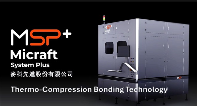
In response to this market momentum, Taiwan-based precision equipment manufacturer Micraft System Plus Co., Ltd. (MSP+) has officially announced the launch of its first self-developed TCB bonder, which will make its public debut at SEMI Taiwan 2025. Purpose-built for heterogeneous integration applications, the system integrates Micraft’s years of expertise in precision automation and features localized heating, programmable temperature control, pressure sensing, platform leveling, and micron-level alignment—marking a new milestone for Taiwan’s equipment industry in advanced semiconductor processes.
According to Micraft, the system employs multiple independently controlled heating modules, enabling rapid localized heating and cooling to minimize the thermal-affected zone and reduce warpage risk. Leveraging its extensive wafer bonder experience with optical semiconductor customers, the company has incorporated pressure sensing and leveling technologies that dynamically adjust bonding pressure and thermal profiles. This ensures uniform bonding quality and high yield, particularly for fine-pitch, low thermal stress, high-precision, and high-throughput packaging requirements.
The bonder is further equipped with advanced optical alignment modules from Carl Zeiss, combined with Micraft’s proprietary optical system and cutting-edge vision algorithms. This enables alignment accuracy of better than 1 μm. In addition, the system offers high process flexibility, supporting a wide range of materials and carrier formats to meet diverse requirements of OSATs and IDMs.
Micraft has long been a pioneer in the MicroLED equipment market, with its laser mass transfer and repair platforms already adopted and mass-produced by Taiwan’s two leading panel makers. By extending its expertise into advanced packaging, Micraft leverages its core strengths in precision motion control, optical integration, and thermal processing. Several leading domestic and international semiconductor customers have already initiated tool qualification programs.
Looking ahead, Micraft plans to continue developing next-generation wafer-level bonding equipment, including Hybrid Bonding and Co-Packaged Optics (CPO), to address the rising demands of 3D IC and chiplet architectures. Through these efforts, Micraft aims to strengthen Taiwan’s role in the global advanced packaging supply chain and further advance the localization and globalization of Taiwan’s precision equipment technologies.
Micraft System Plus warmly invites industry partners to visit its booth at SEMI Taiwan 2025 to explore collaborative opportunities and witness the next generation of bonding solutions.