Thanks to the AI tsunami, demand for AI chips from all sectors is continuing to surge. The Chip-on-Wafer-on-Substrate (CoWoS) architecture that dominates existing 2.5D and 3D packaging technologies is however held back by the number of chips that can be produced on 12" wafers. Demand for AI chips from the explosion of AI applications will therefore continue to outstrip supply for at least the next few years.
The industry is now turning to Panel-level Packaging (PLP) to overcome problems such as low yield and high cost in AI chip production. Increasing the usable wafer area will greatly increase the production output of AI chips. It is true however that many challenges still remain in the commercialization process for PLP, be it the production process or materials.
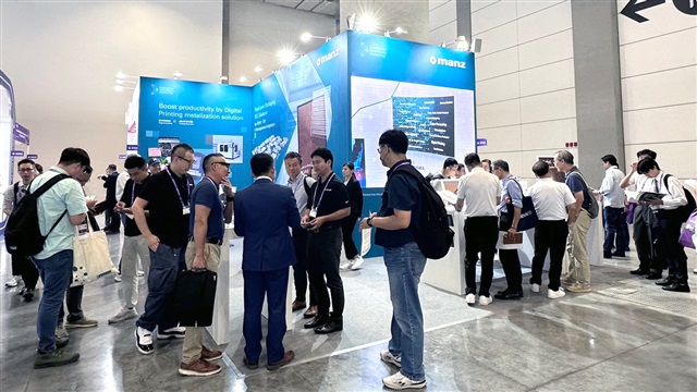
This is why Manz, a PLP pioneer and leading supplier of RDL production equipment, proposed the new Chip-on-Panel-on-Substrate (CoPoS) concept to achieve a breakthrough in production. Manz drew on its many years of experience with PCB, IC substrate, panel, and packaging processes to come up with the "CoWoS panelization" solution. Under the CoPoS packaging architecture, chips are laid out on a rectangular substrate instead of a circular substrate to eliminate a bottleneck in AI chip production.
Panel-level packaging is the key to overcoming the AI chip production bottleneck
Manz Asia General Manager Robert Lin stated that advanced packaging architectures generally have three components : the Chip Layer, Silicon Interposer, and IC Substrate. Continued reductions in IC pin size and line width make finding the right substrate difficult. RDL technology is therefore needed to redistribute pin locations and make lines wider so they can be successfully connected to the PCB. RDL is therefore crucial to improving chip packaging yields.
What future challenges will CoWoS face? As new generations of AI chips appear, the number of dies in a single AI chip package will naturally increase as well. The overall footprint of the packaging will naturally increase. For CoW AI chips of mainstream brands, their footprint will grow by 50x54mm in 2023 all the way to 66x68mm in 2026, and 80x80mm in 2027. The number of AI chipsets produced per 12" wafer will drop from 14 to 11 then 4 in response. The ongoing decline in CoW production output will continue to inflate the production costs of AI chipsets as well.
According to Lin, 700x700mm, 600x600mm or even the smallest 510x515mm panel-level packages all offer several times the usable area of 12" wafers. Chip layouts are also easier to develop for the square substrates. It is therefore not hard to see why IC companies all believe that PLP will be the future and this will create a tremendous opportunity for CoPoS.
Leverage experience with RDL R&D and mass production to overcome the challenges in the PLP process
Under the panelization concept, the interposer in the packaging is produced as panels instead of wafers. The IC substrate is also changed from organic substrate to glass substrate. Intel had previously announced in 2023 that glass will be the next-generation substrate. The Through Glass Vias (TGV) process will be used to form the conductive layer that connects the substrates of the chip's upper and lower circuits. Glass was chosen because it is more resistant to warpage and signal noise than organic substrates, and offers superior thermal dissipation.
Manz is a long-time developer of RDL production equipment and is now developing production equipment for conductive layers on glass substrate. A full set of wet process equipment for cleaning, developing, etching, stripping, and electro-plating has now been progressively developed. Manz is also using its extensive experience to shorten the learning curve for the industry and help them realize the mass production of glass substrates faster.
Transitioning from a circular to square packaging process requires extensive investment in R&D on materials and equipment. Lin believes that since panels have a larger area than wafers and very different production processes, the CoPoS concept is no doubt one of the best solutions to the problem of production capacity; on the other hand, problems such as warpage and evenness must still be overcome to achieve high-definition conductor patterns and this will represent a challenge for yield.
The above challenges highlight the advantages offered by Manz and new opportunities. Manz has been investing in panel-level packaging process equipment for quite some time. The Company has not only accumulated extensive experience with the delivery of mass production solutions but is also familiar with customer concerns regarding warpage and evenness. For this reason, Manz works closely with electroplating solution, glass and other material suppliers to help customers resolve related production issues as quickly as possible. Manz has already developed key production modules for Fan-Out Panel Level Packaging (FOPLP) and TGV that are now being validated by customers for pilot and mass production.
Manz's next move will be to conduct further R&D on breakthroughs in RDL layouts in order to meet customers' exacting requirements on minimization of line width/spacing for AI chips. Manz is aiming for a reduction from 10µm to 5µm or even to 2µm and 1µm in its role as a supporter of advanced processes.

Manz has continued to develop new breakthroughs that will provide customers with even better quality products and services
Photo: Manz
