The rise of artificial intelligence (AI) and the new energy / autonomous vehicle industry presents both challenges and exciting opportunities for the printed circuit board (PCB) and packaging substrate manufacturing business. These dynamics create enormous opportunities and an appetite for fast, efficient, and massive computing resources. The mega-monolithic silicon chip is being replaced by 3D heterogeneous integration of multiple chiplets assembled on an organic build-up substrate platform.
MKS Instruments is leading the way in PCB, package substrate, and many areas of wafer-level packaging. At the TPCA Show Taipei 2024, the company presented a wide range of solutions from its Atotech and ESI Laser Systems brands for the industry, from wet chemical processes and production systems to auxiliary equipment, laser drilling systems, and software solutions, demonstrating their new synergies and expanded capabilities to provide manufacturers with improved production results in terms of higher yield, reliability, and operational efficiency.
In an interview at the MKS booth, Dr. John Lee, President and CEO of MKS Instruments, discusses the company's strategy to help customers design and manufacture specialized PCBs and package substrates for AI and automotive applications, and to scale operations globally. He explains that more than 85% of the semiconductor front-end applications and more than 70% of the critical steps in package substrate and PCB manufacturing use MKS products. "Our enabling technologies are essential to the development of next-generation electronic devices, from semiconductors to advanced printed circuit boards," he notes. The following summarizes what Dr. Lee shared.
Optimize the Interconnect Powering the Future of Electronics
Surround the Wafer and Surround the Workpiece is MKS's key strategy to address the needs of the semiconductor, advanced electronics, and packaging markets by providing customers with the key components, systems, and services to enable the successful implementation of these solutions. As the advanced packaging and heterogeneous integration technologies continue to follow Moore's Law and improve the performance of multiple silicon dies in a single package, high-speed and reliable interconnects between different dies play an important role.
The challenges are many, including multilayer, small alignment, fine line spacing, new materials, and rapid technology upgrades. The industry needs better equipment, tools, and chemistry to meet these needs. MKS has the broadest portfolio of capabilities in the industry and the ability to do it all. The company leverages its expertise in lasers, optics, motion, process chemistry, and equipment to differentiate itself in the marketplace with the ability to Optimize the Interconnect, a key driver for the coming era of advanced electronics, characterized by increasing miniaturization and complexity.
Key MKS Solutions at the TPCA 2024 Show
On the chemistry side, highlights in surface treatment include EcoFlash S300, a new differential etch solution suitable for advanced package substrates, and our new high-tech inner-layer adhesion promoter for high-speed AI applications. For metallization, our highlights include Printoganth MV TP2, a high-performance electroless copper process specifically designed for SAP fine line applications, and our even more enhanced Printoganth MV TP3 process, which enables ultra-thin Cu deposition for fine lines down to 2/2 µm L/S, ideally combined with Cupraganth MV, our new and revolutionary copper-based activation system. For electrolytic copper plating, we highlight our new reverse pulse plating solution for inclusion-free, high aspect ratio through hole filling of package substrate cores, Inpulse 2THF2, and our production-proven InPro SAP3 process for BMV filling with best surface distribution at high current densities. For conformal high-hole density package substrate core plating we are promoting Cuprapulse XP7-IN, our new solution for excellent plating uniformity.
For final finishing, highlights range from the OSP solution OS-Tech SIT 2, the new Aurotech G-Bond 3 versatile gold bath for nickel/gold, nickel/palladium/gold, and palladium/gold plating to Stannatech for flex PCBs, as well as for thick tin plating of µ-LEDs or solder depot plating and Stannatech IC for package substrates.
PCB equipment systems promotions include G-Plate, a new HVM tool for PTH processes of next-generation package substrates enabling the highest yields and cutting-edge fine line capability targeting L/S <5/5 µm, vPlate, a new vertical continuous plating tool for advanced HDI and package substrate for best-in-class surface uniformity. And last but not least the new Uniplate, the company's flagship HVM system and industry-leading horizontal plating equipment for next-generation HDI PCBs and package substrate manufacturing.
Laser equipment promotions include the latest Capstone, a high-performance/throughput productivity breakthrough for flex PCB UV drilling, and Geode (CO2 and UV laser for HDI and package substrate applications). A special show highlight is Geode A, our new CO2 laser system for high-precision and high-speed ABF build-up laminate processing. Geode G2 is our new CO2 laser system for high-precision and high-speed HDI and mSAP via drilling. The Geode platform provides 15% higher optical transmission, 21% less total service area, and up to 65% lower power consumption.
These innovative production solutions and process chemicals, such as the above-listed equipment of the horizontal Uniplate for next-generation HDI PCB and package substrate manufacturing, are not only designed for maximum yield and effective fluid performance but also go a step further to significantly reduce water consumption and increase of energy efficiency.
As another example, as advanced technology in PCBs moves closer to the semiconductor industry, MKS has developed a wide range of solutions for the next generation of package substrates, which use high-end SAP technology requiring less than 5/5µm lines and spaces. These breakthroughs leverage MKS' unique portfolio of combined services in local technical centers, enabling the company to reduce the cycle time for a typical ABF sample from three months or more to less than one month. In addition, MKS is currently working with industry partners to enable 20/20 µm lines and spaces for substrate-like PCBs using mSAP technology.
In addition, MKS supplies several key products for surface treatment, desmear and metallization, electrolytic copper plating, and final finishing to meet the growing demand for FC-BGA and FC-CSP. And the new advances are also being implemented in new materials such as glass substrates and the associated wet chemical processes and manufacturing systems that enable the fine line and high-speed applications of the future of advanced packaging and heterogeneous integration technologies.
This is because MKS offers a one-stop-shop destination for pre-treatment, via formation, plating, and final finishing with fast turnaround times that do not interrupt production, enabling customers to achieve better yields, productivity, and performance.
New expansion to capitalize on opportunities in Southeast Asia
MKS continues to provide industry-leading products and support to customers in the APAC region. There are currently 14 manufacturing facilities in Asia, including China, India, Japan, Korea, Malaysia, Singapore, South Korea, and Taiwan. In addition, MKS has established various locations throughout the region, including R&D and engineering centers, manufacturing plants, tech centers, and sales and service offices.
Much like the semiconductor industry, the printed circuit board, package substrate, and advanced packaging industries are increasingly demanding smaller features, higher density, better performance, and greater manufacturing capacity. The PCB manufacturing landscape in Southeast Asia is undergoing a significant shift, with Thailand quickly becoming the next PCB manufacturing hotspot, attracting significant investment from Chinese, Korean, Taiwanese, and Japanese PCB manufacturers. While cost efficiency has traditionally been a key driver of manufacturing relocation, the market shift to SEA, and Thailand in particular, is being driven primarily by supply chain diversification.
Two major announcements in October 2024 highlight new investments from MKS. Firstly, MKS will begin construction of a new Super Center factory in Penang, Malaysia, to support wafer fabrication equipment manufacturing in the region and globally. With proximity to customers and suppliers and a robust technology infrastructure, MKS has chosen Penang as its home to support strong semiconductor ecosystem partners.
This expansion in Malaysia is an important milestone for MKS as it continues to expand its capabilities as a leader across a wide range of semiconductor manufacturing applications. This Super Center in Malaysia will better serve the APAC semiconductor market and enable MKS to meet the skyrocketing demand for AI, high-performance computing, automotive technologies, and industrial Internet of Things solutions.
A second significant development was the announcement that MKS is opening a technical center and manufacturing facility in Samut Prakan, near Bangkok, Thailand, to serve the growing PCB and package substrate industries in Southeast Asia. Increased competition in the region could lead to accelerated technological advancements in PCB manufacturing, and the emergence of Thailand as a PCB hub could further support the growth of the Southeast Asian electronics sector.
While MKS has a strong presence in SEA today, particularly in Thailand, it is well placed to welcome and serve PCB manufacturers, particularly Chinese companies, overseas. "We will continue to invest in China and build more chemical production facilities to serve Chinese PCB customers. Our deep commitment to APAC is more than just strategic; it is the foundation of our future," said Dr. Lee.
"As semiconductor packaging and heterogeneous integration technologies become more advanced, the need for innovation in PCB and package substrate technology is accelerating. MKS has a well-established and industry-leading presence in APAC and here in Taiwan, with sophisticated equipment process expertise and highly skilled teams of experts. These investments in Asia reflect MKS' commitment to supporting the growth of the semiconductor, PCB, and package substrate markets to drive innovation and to be a key player in the future of technology. We look forward to continuing to invest in Asia's bright future," Dr. Lee concluded.

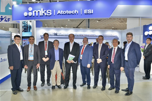
Group picture for John, Gary, and MKS teams

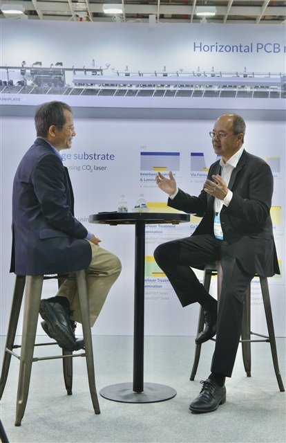
MKS CEO Dr. John Lee interviewed by DIGITIMES Gary Cheng


