Rapidus is expected to begin full-scale production in fiscal 2028. Mass production of 2nm-class chips is scheduled to commence in the second half of fiscal 2027, according to Kyoto News. The company's business plan, submitted to Japan's Ministry of Economy, Trade and Industry, outlines a strategy to enter volume production in late fiscal 2027. The plan calls for expanding output approximately fourfold within the first year of operation.
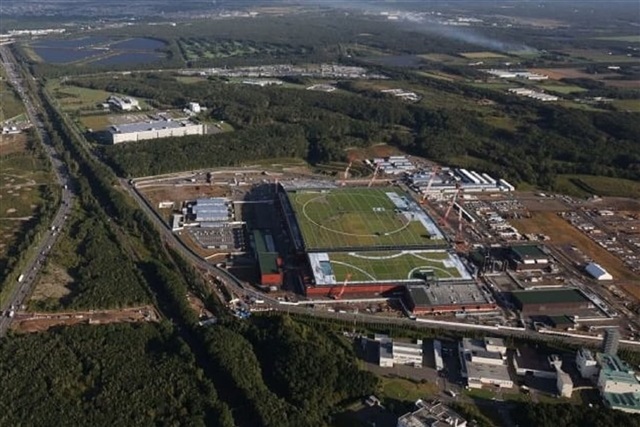
Manufacturing will take place at the Rapidus plant in Chitose, Hokkaido. The company will produce circuit-formed wafers there. At the start of mass production in the second half of fiscal 2027, the company plans an initial monthly output of 6,000 wafers. It intends to increase capacity to approximately 25,000 wafers per month over the following year. The Hokkaido facility is designed to handle both front-end wafer fabrication and back-end processes, including dicing and packaging.
Tool ramp and yield challenges
Production of leading-edge semiconductors requires the simultaneous ramp-up of more than 200 manufacturing tools. Kyoto News reported that improving yield through advanced process control is considered the most difficult hurdle for the company. Yield performance directly affects both chip performance and production costs.
As a contract manufacturer, Rapidus must secure stable orders from customers to maintain plant utilization rates. Achieving high yields and ensuring consistent customer acquisition remain the primary challenges for the company's expansion plan.
Back-end automation strategy
Separately, Nikkei reported that Yasumitsu Orii, Senior Managing Executive Officer and Head of Engineering Center at Rapidus, outlined the company's advanced manufacturing strategy at a February 6, 2026, economic seminar in Kitakyushu.
Orii highlighted "chiplet" technology, which integrates different types of chips onto a single substrate. He said, "We will refine back-end automation technologies and take on the challenge of high-performance, leading-edge semiconductors."
In addition to front-end fabrication, Rapidus plans to operate a pilot back-end line this spring. The line will mount chips onto electronic substrates. Describing progress at the Hokkaido facility, Orii stated, "The front-end and back-end organizations have come together and are moving toward our goals with a seamless manufacturing line."
Nvidia comments on AI in semiconductor manufacturing
In a separate Nikkei interview, Tim Costa, general manager of industrial and computational engineering at Nvidia, discussed GPU applications in semiconductor manufacturing. He said these applications have expanded beyond lithography.
"In the semiconductor field, applications in lithography processes that form circuits have progressed," Costa said. "Nvidia has been providing libraries capable of handling extremely heavy computational methods for several years. Currently, we can accelerate the computational processes required for lithography by up to 70 times."
At TSMC, design simulation calculations have been accelerated by up to 100 times, he said.
Costa added that GPU-accelerated processes have expanded significantly. One to two years ago, these processes were largely limited to lithography. Now they extend to defect detection, inspection, and materials design simulation.
Regarding cooperation with Japanese companies, Costa said Nvidia is already collaborating with firms including Rapidus and Advantest. Initial discussions are underway with a considerable number of other companies.
Rapidus' ability to ramp 2nm production on schedule will depend on several factors. These include achieving high yields, scaling capacity from 6,000 to 25,000 wafers per month, and securing stable customer demand as it brings its Chitose facility into full operation.
Article edited by Jerry Chen