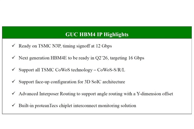
Global Unichip Corp. (GUC), the advanced ASIC leader, today announced the successful demonstration of a 12 Gbps HBM4 IP platform implemented on TSMC's 3nm process technology at the Partner Pavilion of the TSMC 2026 North America Technology Symposium. The platform features GUC's in-house full functional HBM4 Controller and PHY IP, integrated with a partner's HBM4 memory, and used TSMC's industry-leading CoWoS advanced packaging technology.
GUC's previous-generation HBM3E PHY and Controller, deployed in customers'3nm products, have achieved speeds 15% above specification in production. JEDEC continues to drive an aggressive HBM roadmap, increasing memory throughput and capacity while further doubling the data bus width in HBM4. Comparing with HBM3E, GUC's HBM4 IP delivers 2.5x bandwidth, while improving power efficiency by 1.5x and area efficiency by 2x.
In line with GUC's previous HBM, GLink, and UCIe IP solutions, the HBM4 IP integrates proteanTecs' interconnect monitoring solution to provide high visibility for PHY testing and characterizing, while enhancing in-field performance and reliability for end products.
To address the growing demand for 3DIC architectures, GUC's HBM4 PHY also supports a face-up
configuration, enabling integration with TSMC's SoIC face-to-face technology. The PHY macro
integrates TSVs for PHY's I/O signals, power, and ground connections, and also reserves TSVs for
power feedthrough to the top die, supporting the power distribution requirements of the upper logic die.
"We are proud to be the first company to demonstrate a 12 Gbps HBM4 IP to customers at the
TSMC Symposium" said Igor Elkanovich, CTO of GUC. "Together with GUC's UCIe and GLink-
3D IPs, we offer a complete 2.5D/3D IP solution for modern 3.5D system architectures, including
TSMC SoIC-X on CoWoS."
For more information,please visit our website.
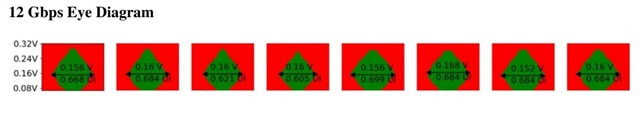
12 Gbps Eye Diagram. Credit:Guc