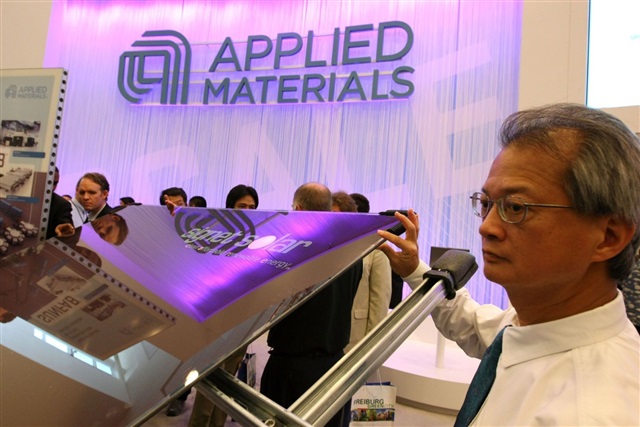
Applied Materials and TSMC have announced a partnership to accelerate semiconductor technologies for AI, aiming to speed commercialization and improve the energy efficiency of chips spanning data centers and edge devices. The collaboration promises global supply chains, cloud services, and device makers faster access to advanced nodes and reduced time from development to high-volume manufacturing.
Building on 30 years of collaboration
Applied Materials said the innovation partnership with TSMC builds on more than 30 years of collaboration and will focus on co-innovating at Applied's EPIC Center in Silicon Valley to advance materials engineering, equipment innovation, and process integration technologies. The companies said the work is intended to deliver energy-efficient performance "from the data center to the edge," addressing demands driven by artificial intelligence and high-performance computing.
Gary Dickerson, president and CEO of Applied Materials, described the move as strengthening a long-standing relationship and accelerating the development of technologies needed to address the rising complexity of the chipmaking roadmap. Dr. Y.J. Mii, executive vice president and co-chief operating officer at TSMC, said that evolving device architectures are increasing demands on materials engineering and process integration, and that industry-wide collaboration is required to meet AI challenges at a global scale.
Where the real work happens
The work at the EPIC Center will target materials engineering innovations for advanced logic scaling, with a focus on process technologies aimed at improving power, performance, and area across leading-edge nodes. The partners have identified the development of new materials and next-generation manufacturing equipment to support the precise formation of complex three-dimensional transistor and interconnect structures, along with advanced process integration approaches to improve yield, variability control, and reliability as devices move toward vertically stacked and more highly scaled architectures.
A US$5 billion bet on the future
Applied noted that as a founding partner of the EPIC Center, TSMC will gain earlier access to Applied's innovation teams and next-generation equipment, which Applied said helps accelerate the path from technology development to high-volume manufacturing. The company described the EPIC Center as a US$5 billion investment — the largest-ever US investment in advanced semiconductor equipment R&D — set to become operationally ready this year and designed to reduce the time required to commercialize technologies from early research to full-scale manufacturing.
Article edited by Jerry Chen


