

Rapidus, Japan's state-backed chipmaker, has developed a prototype glass interposer for artificial intelligence chips. The company says the technology could lower production costs and strengthen its challenge to industry leader TSMC as Japan pushes to rebuild its advanced semiconductor base.
The interposer is a key component in advanced chip packaging. It's the world's first to be cut from a large square glass substrate rather than a conventional silicon wafer, according to Nikkei and company disclosures. Rapidus plans to begin mass production in 2028, integrating the technology into its roadmap for next-generation AI processors.
Cost and scale advantages
Interposers are typically produced from 300-millimeter silicon wafers and used to connect multiple chips within a single package. Rapidus uses a 600-millimeter-by-600-millimeter glass substrate instead. This format significantly reduces material waste and boosts output.
A single glass substrate can yield more than ten times as many interposers as traditional silicon wafers. The larger format also enables production of interposers about 1.3 to 2 times bigger than rivals', allowing more chips to be integrated into one package. Glass offers higher power efficiency than silicon—an increasingly important factor for energy-intensive AI workloads.
Display expertise repurposed
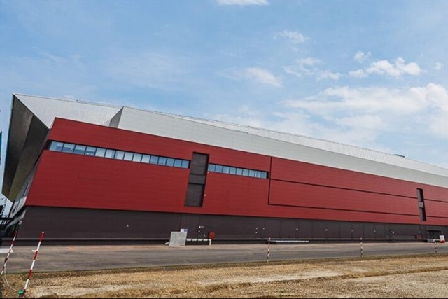
Glass processing poses technical challenges, including fragility during handling and warping risk as substrate sizes increase. To overcome these hurdles, Rapidus recruited former engineers from Japanese display makers such as Sharp. The company began pilot production in June 2025 at a cleanroom facility in Chitose, Hokkaido.
A 600-millimeter substrate is large by semiconductor standards but relatively small in the LCD panel industry. By adapting mature liquid crystal display glass processing techniques for semiconductor use, Rapidus has significantly lowered development barriers.
Industry context
Major chipmakers are also exploring alternatives to silicon substrates. Intel is developing its own glass substrate technology, while TSMC currently mass-produces AI chips using silicon interposers and is advancing other approaches, such as redistribution layer interposers for advanced packaging.
Rapidus senior managing executive officer Yasumitsu Orii said the company's lack of legacy manufacturing constraints allows it to adopt materials best suited for AI chips without being tied to existing processes.
Technology roadmap
Rapidus will showcase the glass interposer prototype starting December 17, 2025, at SEMICON Japan 2025 in Tokyo. President and CEO Atsuyoshi Koike is scheduled to speak during the exhibition.
The company plans to release a process design kit for 2nm chips around March 2026. It aims to begin full-scale production in the second half of fiscal year 2027, which runs from April 2027 to March 2028. According to a business plan submitted to Japan's Ministry of Economy, Trade and Industry, Rapidus targets mass production of 1.4-nanometer chips in fiscal years 2029 to 2030.
Total investment for developing and producing 2nm chips is projected to reach approximately JPY4 trillion (US$25.8 billion). Investments for the 1.4nm technology and subsequent generations are expected to surpass JPY3 trillion.
Government and private backing
The Japanese government has committed cumulative support of about JPY2.9 trillion through fiscal year 2027. It plans to invest an additional JPY100 billion in fiscal year 2025 through the Information-technology Promotion Agency.
On the private side, Rapidus aims to raise about JPY130 billion in fiscal year 2025 and reach a cumulative total of JPY1 trillion by fiscal year 2031. Honda, Fujitsu, and Canon are among the companies that could join Toyota Motor and other existing shareholders as new investors.
Article translated by Sherri Wang and edited by Jerry Chen

